High-Precision PCB & SMT Stencil Manufacturing

Low-Cost, Laser-Cut Stencils with Fast Global Delivery

Get high-precision PCB stencils tailored for your SMT assembly needs. Enjoy low costs, fast turnaround, and global delivery from JHYPCB.

What Are PCB Stencils or SMT Stencils for SMT Assembly?

Essential Tools for Precision SMT Assembly

PCB stencils, also known as SMT stencils, are stainless steel tools used to apply solder paste precisely onto circuit boards for SMT assembly. They ensure accurate paste placement, improving electrical connections and assembly efficiency. With JHYPCB’s laser-cut stencils, you can streamline your PCB assembly process with ease.

  • High-Quality Material: Made from durable stainless steel for long-lasting performance.
  • Precision Application: Designed for accurate solder paste printing in SMT assembly.
  • Framed or Frameless: Choose the best option for your project needs.
  • Custom Solutions: JHYPCB offers stencils that are compatible with all solder-paste printers.
What is the use of PCB stencil?

Why Are SMT Stencils Critical for PCB Assembly?

SMT stencils are essential in PCB assembly, enabling precise solder paste application. They ensure optimal electrical connections, reducing defects during production.

Why choose SMT stencils? They streamline the surface-mount process by allowing accurate paste placement with printers, saving time and costs. JHYPCB’s laser-cut stencils enhance stability and efficiency.

Without stencils, hand-applying solder paste risks inaccuracy and waste. JHYPCB’s stencils guarantee consistent results, ideal for complex assemblies.

  • Precision Printing: Ensures accurate solder paste placement, minimizing defects.
  • Time Efficiency: Speeds up SMT assembly with laser-cut technology from JHYPCB.
  • Cost Savings: Reduces waste compared to manual application.
  • Process Stability: Supports complex PCB designs with consistent results.
SMT Stencil

How to Use PCB Stencils for SMT Assembly?

Using a PCB stencil with JHYPCB ensures precise solder paste application for SMT assembly. Follow these steps to achieve high-quality results:

The Components of the SMT Stencil

Components and structure of PCB Stencil

Solder Paste
Step1: Prepare the Solder Paste:

  • Store unopened solder paste in a constant temperature and humidity freezer.
  • Let it reach room temperature before use for optimal consistency.
  • Stir the paste for 3-5 minutes to ensure even texture.

Soldering Paste Printing with SMT Stencil

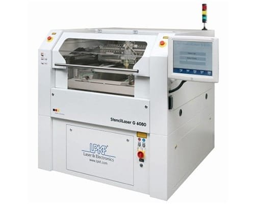
Step2: Perform Solder Paste Printing:

  • Maintain printer conditions at 25±3℃ and 40-70% RH for best results.
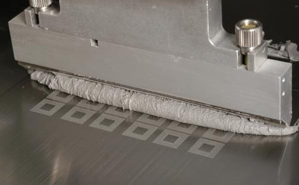
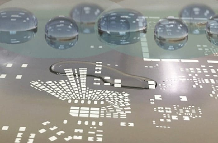
  • Adjust squeegee pressure to ensure clear edges, flat surfaces, and proper thickness.
  • Set squeegee speed to 10-20mm/s, allowing solder paste to roll smoothly.

Reflow Oven

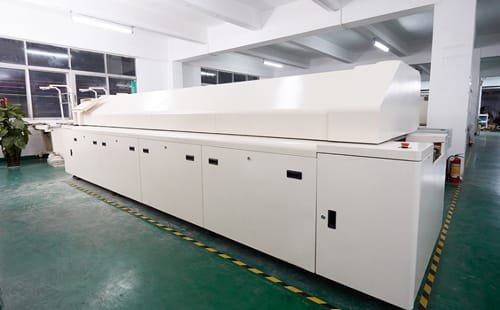
Step3: Use the Reflow Oven:
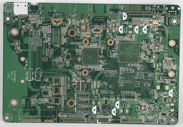
SMT Stencil Design Guide by JHYPCB for PCB Assembly

Designing an SMT stencil ensures precise solder paste application for PCB assembly. Following the IPC-7525 standard, JHYPCB helps you create stencils that release paste smoothly onto PCB pads, improving quality and efficiency.

Key Elements of SMT Stencil Design

  • Data Format: Ensure compatibility with manufacturing software.
  • Process Method: Define laser-cutting or etching techniques.
  • Material: Use high-quality stainless steel for durability.
  • Thickness: Select 0.1mm to 0.15mm for fine-pitch components.
  • Framework: Choose framed or frameless based on your printer.
  • Printing Format: Match PCB layout for accurate paste application.
  • Aperture: Design openings for precise solder paste release.
  • Other Requirements: Include fiducial marks for alignment.

Data Preparation for SMT Stencil Design

Before designing your SMT stencil, prepare the following data to ensure a seamless process with JHYPCB:

With PCB Layout File:

  • Pad Layer (PADS): Include Mark points for SMD components.
  • Silkscreen Layer (SILK): Match the SMD pad positions.
  • Top Layer (TOP): Show the PCB frame outline.
  • Panelization (if applicable): Provide a panelization diagram.

Without PCB Layout File:

  • PCB Prototype or Scanned Image: Include Mark points, PCB shape, and SMD pad positions.
  • Panelization File (if applicable): Specify panel layout.
  • Printing Surface: Clearly indicate the printing side.

SMT Stencil Thickness Design Guide by JHYPCB

SMT stencil thickness, crafted from stainless steel, controls solder paste release to avoid bridging or weak joints. JHYPCB’s design ensures optimal PCB assembly quality.

How to Choose the Right SMT Stencil Thickness

The ideal stencil thickness depends on your PCB components. JHYPCB recommends:

Component PitchRecommended ThicknessBenefits
0.020” (SOICs)0.001” – 0.003”Thin paste for fine-pitch accuracy
0.050” (SOICs)0.004” – 0.007”Thick paste for strong joints

Standard thickness (0.004” – 0.007”) suits most PCB boards, ensuring balanced solder paste application.

Nano-Coating for Enhanced Thickness Design

JHYPCB applies nano-coating to stencil surfaces, improving solder paste release for fine-pitch components like QFN, ICs, BGAs, and 0201 types. This factory-treated feature ensures precision with thinner stencils.

The thickness of the paste stencil for solder ranges from 0.001” to 0.003”

How to Calculate SMT Stencil Thickness

Accurate stencil thickness ensures the right solder paste volume for quality PCB assembly. JHYPCB suggests:

  • Determine Component Needs: Assess pad size and pitch (e.g., 0.020” for fine-pitch).
  • Apply Formula: Thickness ≈ (Pad Area × Paste Volume) / Aperture Area. Consult JHYPCB for precise values.
  • Verify Material: Use stainless steel thickness (0.001” – 0.007”) based on calculation.

Contact JHYPCB for tailored thickness calculations to optimize your design.

Calculation formula of PCB stencil thickness
The PCB stencil opening

Types of PCB Stencils for SMT Assembly by JHYPCB

JHYPCB offers flawless SMT stencils for seamless PCB assembly. Our advanced laser-cutting technology and expert technicians ensure high-quality stencils at competitive prices, tailored to your needs.

Prototype PCB Stencil

Ideal for low-volume manual printing, JHYPCB’s prototype stencils are perfect for quick PCB prototyping.

  • Precision Printing: Reduces errors compared to hand soldering.
  • Time-Saving: Quick alignment speeds up assembly.
  • Cost-Effective: Affordable for small runs without machines.
  • Easy to Use: Simple alignment for repeatable results.
Prototype PCB Stencil

High Precision Laser-Cut SMT Stencil

JHYPCB’s laser-cut stencils, made from 100% stainless steel, offer high precision for various SMT applications.

  • High Accuracy: Ensures precise solder paste application.
  • Fast Delivery: 24-hour turnaround time.
  • Versatile Use: Suitable for fine-pitch and Micro BGA components.
  • Demoulding Ease: Trapezoid openings improve paste release.
Laser-cut SMT stencil

Framed SMT Stencils (Glue-in)

Designed for high-volume printing, JHYPCB’s framed stencils ensure durability and accuracy.

  • Durable Frame: Double-bonded for long-term use.
  • Smooth Apertures: Clean laser-cut walls for excellent printing.
  • High Volume: Ideal for large-scale PCB production.
  • Fast Turnaround: 24-hour delivery standard.
Framed PCB Stencil

Frameless SMT Stencils (Foils)

JHYPCB’s frameless stencils offer flexibility for both universal frames and hand printing.

  • Cost-Effective: More affordable than framed stencils.
  • Space-Saving: Easy to store, eco-friendly design.
  • Versatile Printing: Compatible with machines or hand printing.
  • Precision for Small Runs: Perfect for 16 Mil pitch and Micro BGAs.
Frameless PCB Stencil

Other SMT Stencil Types by JHYPCB

We also provide advanced options to meet diverse needs:

Nano SMT Stencil

Compare JHYPCB SMT Stencil Types

Choose the right stencil for your PCB assembly needs with this comparison.

Stencil TypeBest ForPrecisionCostDelivery Time
Prototype StencilLow-volume prototypingModerateLow24 hours
Laser-Cut StencilGeneral SMT useHighModerate24 hours
Framed StencilHigh-volume productionHighHigher24-48 hours
Frameless StencilSmall runs, eco-friendlyModerate-HighLow24 hours
PCB Assembly Stencil

SMT Stencil Gallery

How to make PCB stencil?

SMT Stencil Manufacturing Videos

High-Speed Laser Cutting of SMT Stencils

Laser-Cutting of SMT Stencils with Lowest Investment Cost

SMT Prototype Stencil Printing – Hand Printing of a Prototype Stencil

SMT Stencil Manufacturing by JHYPCB for PCB Assembly

JHYPCB excels as an SMT stencil manufacturer, using advanced laser cutters and skilled technicians to deliver high-quality stencils for PCB assembly at competitive prices.

How to Order PCB Stencils from JHYPCB

JHYPCB simplifies stencil ordering with flexible data formats. We accept:

  • PCB Design File: *.PCB format for direct input.
  • Gerber/CAM File: Exported from PCB files for precision.
  • CAD Files: *.DWG or *.DXF formats for compatibility.

Required PCB layers include:

  • Circuit Layer: Provides complete SMT stencil data.
  • Silkscreen Layer: Confirms component type and printing surface.
  • SMT Layer: Defines stencil aperture layout.
  • Solder Mask: Identifies exposed pad positions.
  • Drilling Layer: Marks plug-in component locations.

SMT Stencil Fabrication Process by JHYPCB

JHYPCB offers three advanced methods to create high-quality SMT stencils:

  1. Chemical Etching:
    • Process: Data file → Film → Exposure → Development → Etching → Cleaning → Netting
    • Benefits: Fast production and low cost, ideal for quick projects.
  2. Laser Cutting:
    • Process: Film → Coordinates → Data processing → Laser cutting → Polishing → Netting
    • Benefits: High precision, trapezoidal openings for easy demoulding, moderate price.
  3. Electroforming:
    • Process: Photosensitive film coating → Exposure → Development → Electroforming nickel → Routing → Cleaning → Netting
    • Benefits: Smooth hole walls, perfect for ultra-fine pitch stencils.
SMT Stencil Fabrication Process

SMT Stencil Production and Testing Equipment

SMT Stencil Laser cutting Workshop
SMT Stencil Production Workshop-1
SMT Stencil Production Workshop-2
SMT Stencil Production Workshop-3
SMT Stencil Production Workshop-4
SMT Stencil Production Workshop-5
SMT Stencil Production Workshop-6
SMT Stencil Closure Workshop
Professional SMT Stencil Design Software
Nano Stencil Coating Machine
100 times magnifying glass
Check with a magnifying glass
Automatic Stencil Detector
Nano SMT Stencil Wear Tester
SMT Stencil Laser Cutting Machine
Online polishing machine

How to store and pack PCB stencils?

Finished SMT Stencil
Stencil packaging protected by wooden planks
Laser SMT Stencil for Delivery
SMT Stencil To Be Delivered

JHYPCB: Best SMT Stencil Manufacturer for PCB Assembly

JHYPCB delivers top-quality SMT stencils for seamless PCB assembly. Our stencils are 100% laser-cut from type 304 stainless steel, ensuring the finest finish on the market.

With a 0.001″ laser beam and 98% overlap, we achieve smooth aperture walls for optimal solder paste release—unlike competitors’ 0.003″ lasers that leave “mouse bites.” Choose from prototype, frameless foil, or framed stencils, available in various sizes to fit your printer and project needs.

PCB Stencil FAQs by JHYPCB for SMT Assembly

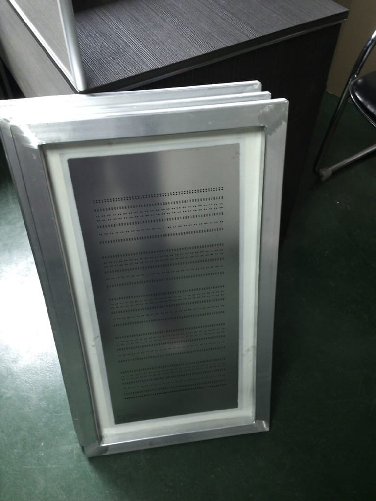
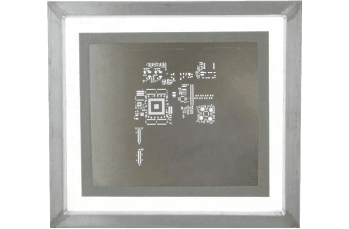
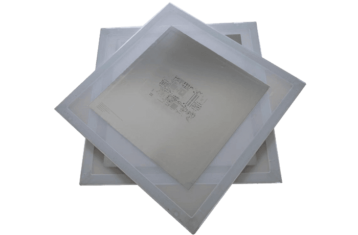
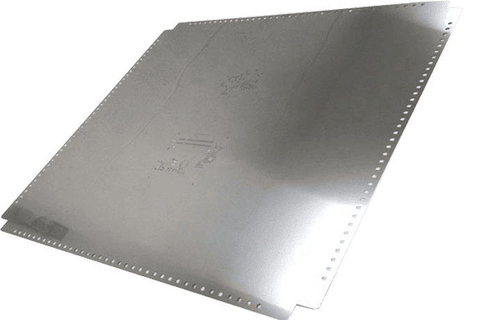
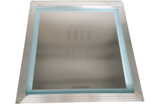
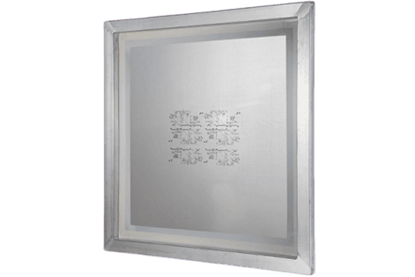
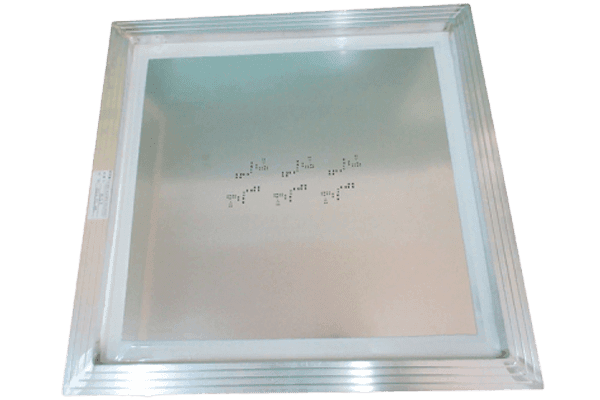
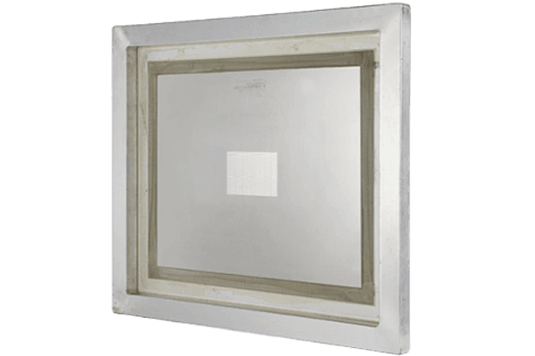
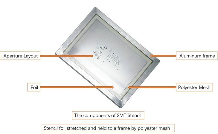
Framed stencils feature a 0.5″-1.5″ metal frame, ideal for large-scale production with automated printers. Frameless stencils are thin sheets, perfect for manual use or small runs.

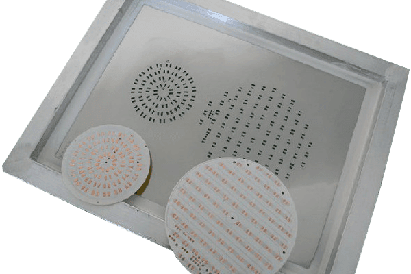
JHYPCB uses type 304 stainless steel (0.0007″ laser spot, 0.001″ aperture) for superior precision and paste release. Polyimide (0.003″ spot, 0.005″ aperture) suits limited uses for 0402+ components but lacks stainless steel’s flatness and durability.

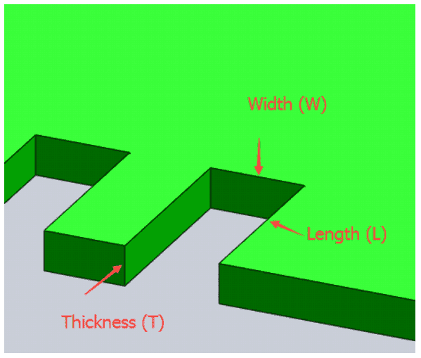
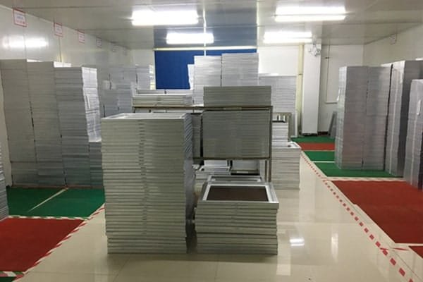
Stencil size includes internal (PCB-compatible) and overall (printer-compatible) dimensions. For a 50x50mm PCB, framed stencil size is ~150x150mm, frameless is ~250x250mm. JHYPCB supports 650x650mm or 736x736mm overall sizes.

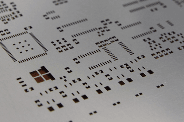
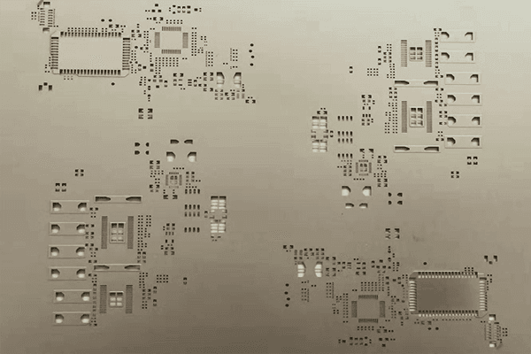
Choose based on pitch: 0.13mm/0.12mm for QFP ≤ 0.5mm, 0.15mm-0.20mm for > 0.5mm, 0.15mm for BGA > 1.0mm, 0.13mm for 0.5mm-1.0mm BGA.

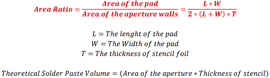
The stencil aperture matches PCB land areas, with a 90%-100% pad-to-aperture ratio recommended at 0.125mm thickness for optimal paste application.

SMT stencil wipes, made from wood pulp and polyester, remove excess paste and glue, reducing scrap rates. They suit all major printers like MPM and DEK, enhancing efficiency.

SMT Stencil Wipes

Features of SMT stencil wipes

SMT stencil wipes have the characteristics of durable, soft, dust-free, roll shape, strong tensile strength, efficient water and oil absorption, and anti-static.

SMT stencil wipes apply to SMT production lines, semiconductor assembly lines, optical products, PCB products, medical equipment, etc. It is advantageous for SMT factories to remove excess solder paste and red glue on the SMT stencil and circuit boards and keep circuit boards clean to reduce the scrap rate significantly and vastly improve production efficiency and product quality. To improve work efficiency, save expenses, and effectively control the dosage of SMT stencil wipes, the width and length of wipes can be selected according to the actual use.

SMT stencil wipes apply to all automatic solder paste printing models such as MPM, DEK, KME, Yamaha, Minami, JUKI, ekra, Panasert, Fuji, Sanyo, etc.

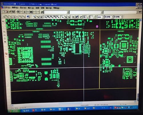
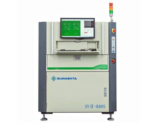
Provide: production requirements, stencil type (solder/red glue), polishing (polishing/electrolytic), PCB file (GERBER, CAD, etc.), size, frame type, thickness (based on smallest pitch), and lead/lead-free status.

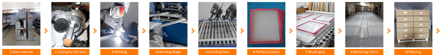
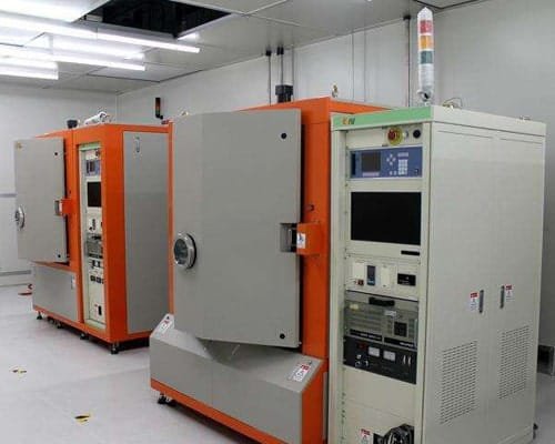
Key factors include fabrication process, materials, opening design, production accuracy, usage, cleaning, and storage conditions.

JHYPCB primarily uses type 304 full-hard stainless steel for its durability and precision (0.0007″ laser spot, 0.001″ aperture). We also offer polyimide for specific low-volume needs, though it’s less precise (0.003″ spot, 0.005″ aperture). Contact us for material recommendations tailored to your project.

JHYPCB offers rapid delivery: prototype and laser-cut stencils in 24 hours, framed stencils within 24-48 hours depending on complexity. Contact us for exact timelines based on your order.

Yes, JHYPCB provides fully customized stencil designs based on your GERBER, CAD, or PCB files. We adjust aperture sizes, thickness, and frame types to meet unique project requirements. Request a consultation today!

Clean your JHYPCB stencil with isopropyl alcohol and a soft brush after use to remove solder paste. Store it flat in a dry, dust-free environment to maintain quality. Avoid stacking to prevent damage.

Check stencil alignment, thickness, or aperture design if you encounter printing issues (e.g., uneven paste or bridging). Contact JHYPCB’s support team for troubleshooting or a replacement if defective.

Scroll to Top