SMT PCB Assembly – Component Package, Defect & DFM Guide
Surface mount technology is the backbone of modern PCB assembly — enabling smaller boards, higher component density and faster automated production. PCBELEC helps you understand SMD package options, common assembly defects, and design best practices before you start your project.
SMT assembly involves more than placing components on a board. The package type you choose affects solder joint reliability, the stencil design, and the reflow profile. Understanding common defects helps you catch problems early, and following DFM best practices reduces rework, cost and lead time.
SMD Component Package Types: A Selection Guide
Choosing the right SMD package affects board size, assembly cost, solder joint reliability and inspection difficulty. The tables below summarize the most common passive and active SMD packages used in SMT PCB assembly.
Passive Component Packages (Resistors, Capacitors)
| Package | Dimensions (Metric) | Typical Application | Assembly Difficulty | Notes |
|---|---|---|---|---|
| 01005 | 0.4 × 0.2 mm | Ultra-compact mobile devices | Very High | Requires specialized equipment; limited to high-density designs |
| 0201 | 0.6 × 0.3 mm | Compact consumer electronics | High | Common smallest size for most SMT lines |
| 0402 | 1.0 × 0.5 mm | General-purpose compact boards | Medium | Widely used; good balance of size and handling |
| 0603 | 1.6 × 0.8 mm | Most common SMT applications | Low | Most popular passive package; easy to place and inspect |
| 0805 | 2.0 × 1.25 mm | Power resistors, larger capacitors | Low | Used where higher power rating or capacitance is needed |
| 1206 | 3.2 × 1.6 mm | High-power resistors, decoupling caps | Low | Larger footprint; used for power and filter applications |
Active Component Packages (ICs, Transistors, Connectors)
| Package | Lead Pitch | Typical Application | Inspection Requirement | Notes |
|---|---|---|---|---|
| QFP (TQFP, LQFP) | 0.3–0.65 mm | Microcontrollers, processors | AOI | Visible leads; moderate placement precision needed |
| QFN / DFN | 0.4–0.65 mm | Compact ICs, power management | AOI + X-Ray | Leadless; hidden solder joints require X-ray |
| BGA / µBGA | 0.25–1.0 mm | High-pin-count processors, FPGAs | X-Ray (mandatory) | Solder balls hidden under package; X-ray essential |
| LGA | 0.65–1.0 mm | Socket-style replacement, connectors | X-Ray | Similar to BGA; pads make direct contact |
| SOT-23 / SOT-223 | — | Discrete transistors, diodes | AOI | Small package for 3-terminal devices |
| SOIC / TSSOP | 0.5–1.27 mm | General-purpose ICs | AOI | Common mid-density logic packages |
Key Takeaway: Smaller packages (01005, 0201) enable higher density but require advanced placement equipment and tighter process control. Leadless packages (QFN, BGA, LGA) require X-ray inspection because solder joints are hidden under the component. Always confirm your assembly partner supports your specific package type before ordering.
Common SMT Assembly Defects: Causes and Prevention
Even with automated SMT lines, defects can occur. Knowing the most common failure modes helps you design for manufacturability and know what to inspect. Below are the six most frequent SMT defects, their root causes, and how to prevent them.
Common Defects
- Solder Bridges — Excess solder paste causes adjacent pads to short-circuit
- Tombstoning — Uneven solder paste volume pulls small two-terminal components upright
- Misalignment — Component shifts during reflow due to incorrect pick-and-place data or paste tackiness
- Solder Voids — Trapped air/gas creates cavities in BGA and QFN solder joints, weakening reliability
- Insufficient Solder — Stencil opening too small or paste deposit too thin; weak or open joints
- Cold Solder Joints — Reflow temperature too low; dull, grainy joints with poor electrical connection
Prevention
- Prevention: Reduce stencil aperture, optimize paste viscosity, verify stencil thickness
- Prevention: Ensure even paste deposition via SPI; check reflow ramp rate for uniform heating
- Prevention: Verify CPL/XY data accuracy; ensure adequate paste tackiness before reflow
- Prevention: Optimize reflow profile vacuum phase; use vacuum-compatible paste formulation
- Prevention: Verify stencil aperture design; check squeegee pressure and speed; use SPI
- Prevention: Calibrate reflow oven temperature zones; verify thermal profile against paste spec
Key Takeaway: Most SMT defects originate from solder paste printing and reflow profiling — the two most critical process stages. Solder Paste Inspection (SPI) and Automated Optical Inspection (AOI) catch the majority of these defects before boards leave production. Designers can reduce defect risk by following DFM guidelines for component spacing, pad geometry and thermal relief.
DFM Best Practices for SMT PCB Assembly
Design for Manufacturing (DFM) is the process of optimizing your PCB layout to reduce assembly defects, simplify inspection and lower production cost. Following these best practices before sending files to production helps avoid rework and shorten lead times.
Layout Best Practices
- Component spacing — Maintain minimum spacing between SMD components per IPC guidelines; too-close placement causes solder bridges and makes rework difficult
- Pad geometry — Use NSMD (non-solder mask defined) pads for BGA to improve joint reliability; use SMD (solder mask defined) pads for high-stress applications
- Fiducial marks — Place global fiducials on board corners and local fiducials near fine-pitch components (QFP, BGA) for accurate pick-and-place alignment
- Thermal relief patterns — Use thermal relief pads for large copper areas to ensure even solder heating and prevent cold joints
- Component orientation — Align similar components in the same direction to speed up pick-and-place and improve AOI accuracy
Stencil & Solder Mask Guidelines
- Stencil thickness — 0.12–0.15 mm for fine-pitch (0201, QFN, BGA); 0.15–0.20 mm for standard components
- Stencil aperture design — Reduce aperture area for tight-pitch pads; over-aperture causes solder bridges
- Solder mask clearance — Maintain 50–75 µm clearance around copper pads; insufficient clearance causes paste wicking
- Solder mask color — Use any color, but note that AOI accuracy is optimized for standard green; unusual colors may require calibration
Panelization & Handling
- Panel design — Panelize small boards for efficient SMT processing; use V-scoring or tab-routing for clean depaneling
- Tooling holes — Include 3–4 mm tooling holes at panel corners for fixture alignment
- Fiducial placement on panel — Add panel-level fiducials outside individual board images for machine calibration
- Edge clearance — Keep components at least 3 mm from panel edges and V-score lines to prevent damage during depaneling
Key Takeaway: DFM review before production is the single most cost-effective way to reduce SMT assembly defects. A 30-minute engineering review can prevent hours of rework, missed deadlines and field failures. Always request a DFM check from your assembly partner before approving production.
SMT PCB Assembly FAQs
Still have questions about your SMT PCB assembly project? Below are some of the most common topics customers ask before requesting a quote.
The most common passive SMD packages are 0603 and 0402 for general-purpose boards, with 0805 and 1206 used for power and filter components. For compact and high-density designs, 0201 and 01005 are used. For active components, QFN, QFP, BGA and SOIC are the most common package types. The package size affects placement precision, stencil design and inspection method — smaller and leadless packages require tighter process control and X-ray inspection.
The most frequent SMT defects are solder bridges (excess paste between adjacent pads), tombstoning (uneven heating lifts small components), misalignment (component shift during reflow), solder voids (trapped gas in BGA/QFN joints), insufficient solder (thin paste deposit) and cold solder joints (reflow temperature too low). Most defects originate from solder paste printing and reflow profiling — the two most critical process stages.
DFM (Design for Manufacturing) review is an engineering check of your Gerber files, BOM and assembly data to identify manufacturability risks before production starts. It catches issues like component spacing violations, pad geometry problems, missing fiducials and stencil aperture concerns. A DFM review reduces rework, shortens lead time and improves first-pass yield — it is the most cost-effective quality step in the SMT assembly process.
Yes. SMT assembly supports both single-sided and double-sided boards. Double-sided SMT assembly typically uses a two-stage reflow process: components are placed and reflowed on the primary side, then the board is flipped, components are placed on the secondary side, and the board passes through reflow again. The secondary side uses higher-temperature solder paste or adhesive to prevent components from falling off during the second reflow.
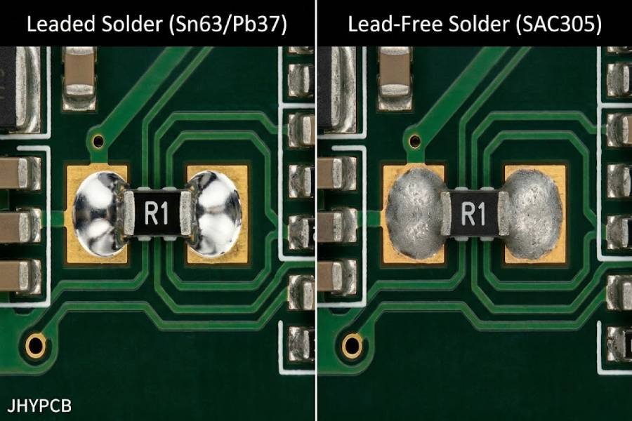
SMT assembly uses solder paste classified by particle size (Type 3, 4, 5) and alloy type. Type 3 (25-45 µm) is standard for most applications. Type 4 (20-38 µm) is used for fine-pitch and small packages (0201, QFN). Type 5 (15-25 µm) is used for ultra-fine-pitch and 01005 components. Common alloys include Sn96.5Ag3.0Cu0.5 (lead-free SAC305) and Sn63Pb37 (leaded). No-clean paste is most common; water-soluble paste is used when post-assembly cleaning is required.
Most standard SMT lines handle down to 0201 (0.6 × 0.3 mm) and 0402 (1.0 × 0.5 mm) components with reliable quality. 01005 (0.4 × 0.2 mm) requires specialized high-precision placement equipment and tighter process control. For fine-pitch active components, 0.25 mm pitch BGA and QFN packages are commonly handled. Always confirm your assembly partner's specific capability range for the smallest component and finest pitch before finalizing your BOM.