PCB Fabrication Process: Step-by-Step Guide to PCB Manufacturing
Explore how multilayer and double-sided PCBs are fabricated, with process diagrams and explanations of the key manufacturing stages. Follow the workflow from engineering review to final inspection, and see how each stage contributes to the finished bare board.
Quick Answer: What Is the PCB Fabrication Process?
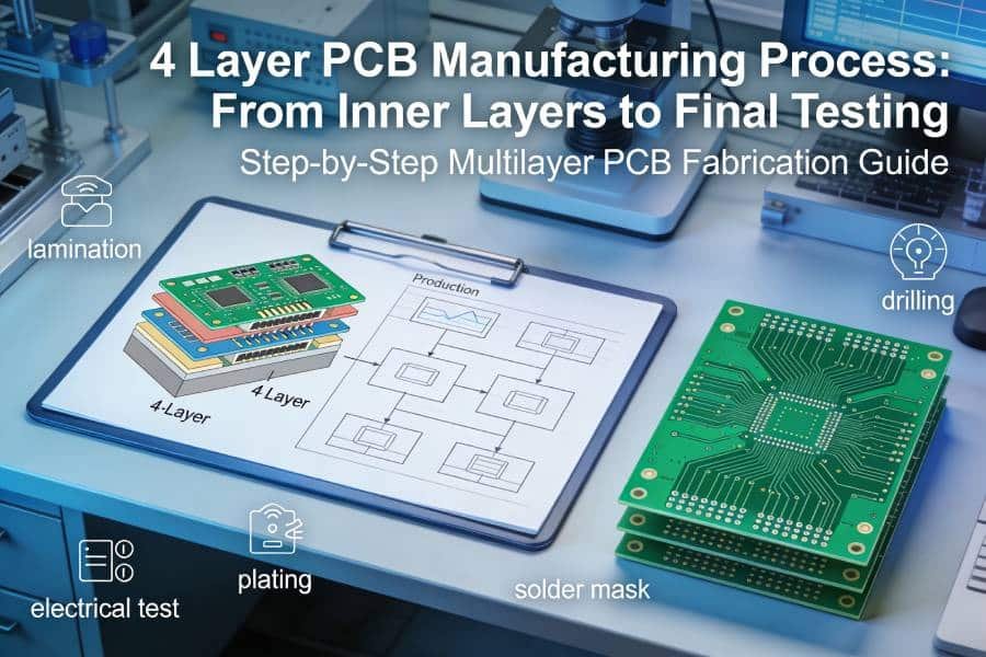
PCB fabrication is the process of turning a PCB design into a physical multilayer or double-sided circuit board. The main PCB manufacturing process steps include pre-production engineering, material cutting, inner-layer imaging and etching, layer stack-up and lamination, CNC drilling, PTH and copper plating, outer-layer imaging and pattern plating, solder mask application, surface finish, silkscreen printing, profiling, electrical testing, and final quality inspection.
Upload your Gerber files for a DFM review, lead-time estimate, and PCB fabrication quotation.
PCB Fabrication Process Overview
A PCB fabrication process flow chart provides a clear view of how a PCB design becomes a finished bare board. The process is divided into sequential stages, each with specific engineering, material, and quality-control requirements. For multilayer PCBs, inner-layer processing and lamination occur before drilling and outer-layer fabrication.
PCB Fabrication Process Flow Chart
The following PCB fabrication process flow chart shows the main manufacturing stages for double-sided and multilayer PCBs. The exact sequence may vary depending on board construction, layer count, material selection, surface finish, and special requirements such as impedance control, heavy copper, or blind and buried vias.

View Full-Size PCB Fabrication Flow Chart
Main Stages of the PCB Manufacturing Process
| Stage | Purpose | Key Output | Typical Quality Control |
|---|---|---|---|
| Pre-production engineering | Review Gerber files, stack-up, drill data, and manufacturability | Manufacturing instructions and production panel design | DFM review, data verification |
| Material preparation | Cut copper-clad laminate and prepreg to production size | Prepared inner-layer cores and bonding materials | Material certification, thickness check |
| Inner-layer processing | Form internal circuit patterns on copper-clad cores | Etched and inspected inner layers | AOI, line-width inspection |
| Oxide treatment and lamination | Prepare copper surfaces and bond layers into a multilayer panel | Laminated multilayer panel | Registration, thickness, and bonding inspection |
| Drilling and PTH | Create holes and establish electrical connections between layers | Drilled and copper-plated holes | Hole inspection, plating thickness check |
| Outer-layer processing | Form external circuit patterns, pads, and traces | Finished outer-layer circuitry | AOI, plating and etching inspection |
| Solder mask and legend | Protect copper surfaces and add component identification | Coated and marked PCB panel | Solder-mask adhesion, legend inspection |
| Surface finish | Preserve solderability and protect exposed copper | Finished PCB surface, such as ENIG, HASL, or OSP | Solderability and thickness inspection |
| Profiling and routing | Cut individual PCBs from the production panel | PCBs with final outline and edge quality | Dimensional inspection |
| Electrical testing and FQC | Verify electrical continuity and final board quality | Approved bare PCBs ready for shipment | E-test, visual inspection, final QC |
Each stage must be controlled to maintain dimensional accuracy, layer registration, copper integrity, hole reliability, solderability, and electrical performance. A well-controlled PCB fabrication process reduces the risk of open circuits, shorts, delamination, poor hole-wall plating, misregistration, and solderability problems.
Detailed PCB Fabrication Process: Step-by-Step
The following sections explain how a typical multilayer PCB is fabricated, from pre-production engineering through inner-layer processing, lamination, drilling, plating, surface finishing, and final inspection.
1. Pre-Production Engineering
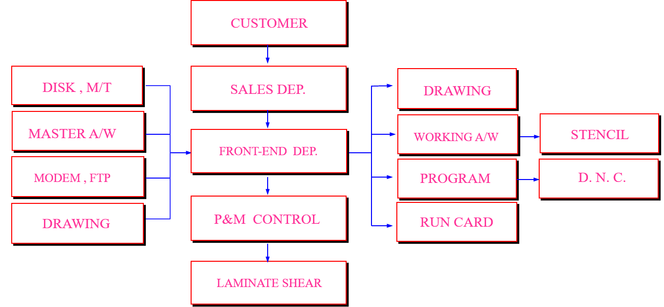
Pre-production engineering is the first stage of the PCB fabrication process. The engineering team reviews the customer’s Gerber files, drill files, stack-up requirements, board outline, copper weights, impedance requirements, and special manufacturing notes before production begins.
During this stage, engineers check whether the design can be manufactured reliably and confirm key production parameters, including layer count, material type, finished thickness, minimum trace and space, hole size, annular ring, surface finish, and tolerance requirements. Any potential manufacturability issues are identified and communicated before the job is released to production.
The output of pre-production engineering is a complete set of manufacturing instructions and a production-ready work plan. Careful engineering review helps prevent misregistration, incorrect stack-ups, drilling errors, and unnecessary production delays.
2. Multilayer PCB Inner-Layer Manufacturing Process

Multilayer PCB inner-layer manufacturing forms the internal copper circuits before the layers are bonded into a single board. The main stages include core preparation, circuit imaging, developing, etching, photoresist stripping, and automated optical inspection (AOI).
Copper-clad cores are cut to production size, cleaned, and coated with photoresist. The circuit pattern is transferred using film-based exposure or direct imaging. Developing removes the selected areas of photoresist, and etching removes the unprotected copper. The remaining resist is then stripped, leaving the inner-layer traces, pads, and copper planes.
AOI checks the etched circuit patterns against the design data before the layers are enclosed by lamination. Inspected cores then receive a surface treatment to promote bonding and are arranged with prepreg and copper foil according to the approved stack-up.
During lamination, controlled heat and pressure bond the stack into a multilayer panel. Drilling and hole metallization follow to create the required electrical connections between layers. Accurate inner-layer processing and registration are essential for keeping the internal circuitry aligned with the subsequent drilling pattern.
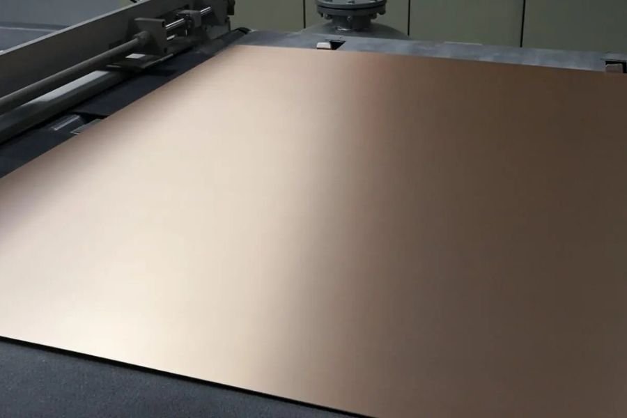
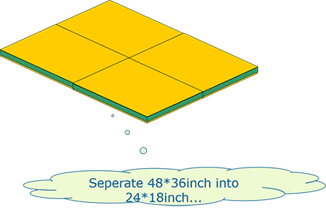
PCB material preparation begins with selecting copper-clad laminate (CCL) that matches the approved stack-up and manufacturing instructions (MI). For multilayer inner-layer cores, the specified laminate type, core thickness, and copper thickness provide the starting point for subsequent circuit imaging and layer bonding.
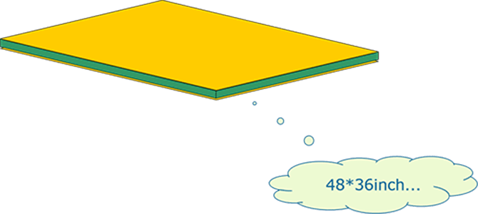
The laminate sheets are cut into production panels sized for the factory’s processing equipment and panel layout. Panel dimensions account for the board arrangement and the space required for tooling and registration features. The illustration below shows an example of dividing a larger laminate sheet into smaller production panels; actual sheet and panel sizes vary with the material format and manufacturing requirements.
Inner-Layer Image Transfer Overview
Inner-layer image transfer defines the copper circuit pattern on each prepared core. After the copper surfaces are cleaned, a photosensitive dry-film resist is applied. The circuit artwork is transferred to the resist through UV exposure using a phototool, or by direct imaging. In a typical negative-working dry-film process, the exposed resist hardens over the copper features that must remain, while developing removes the unexposed resist to reveal the copper that will be etched away.
Etching removes the unprotected copper, and stripping removes the remaining resist, leaving the inner-layer traces, pads, and copper planes. The completed patterns are checked by automated optical inspection (AOI) before bonding preparation, lay-up, and multilayer lamination. The following sections explain the individual stages of this process in more detail.
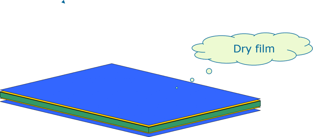
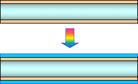
2.2. Inner-Layer Dry-Film Lamination
Dry-film lamination applies a photosensitive resist to the cleaned copper surfaces of the inner-layer core. Before application, the copper is cleaned and prepared to remove oxidation and surface contamination that could interfere with resist adhesion. The dry film is then laminated onto the copper using controlled heat and pressure, forming a uniform coating for circuit imaging.
Consistent adhesion and coverage help prevent defects during exposure, developing, and etching. The laminated surfaces should be free from trapped air, wrinkles, and particles that could disrupt the circuit pattern. The prepared core is then ready for the next stage: inner-layer exposure.
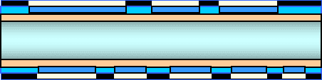
2.3. Inner-Layer Exposure
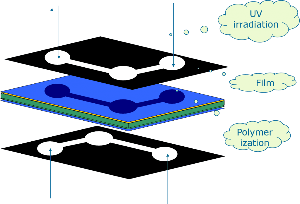
Inner-layer exposure transfers the circuit artwork onto the dry-film photoresist covering the copper-clad core. In a film-based process, the phototool is accurately aligned with the panel, and UV light passes through its transparent areas to expose the resist. Direct imaging provides an alternative by exposing the circuit pattern without a physical phototool.
With the negative-working dry film typically used for inner-layer processing, the exposed areas harden and become resistant to the developer. These areas protect the copper traces, pads, and planes that must remain after etching. Accurate alignment and controlled exposure help maintain circuit dimensions and prepare the resist pattern for developing.
2.4. Inner-Layer Developing
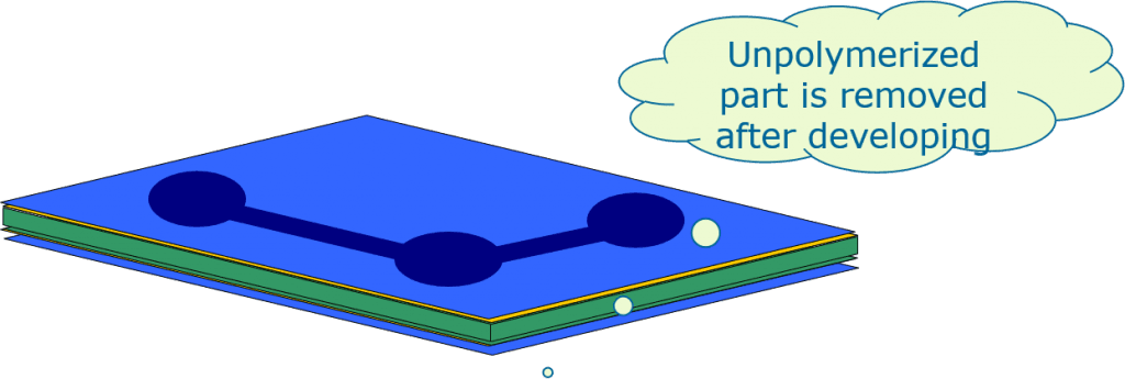
Inner-layer developing removes the unexposed areas of the negative-working dry-film resist after exposure. A controlled developer solution dissolves these areas, revealing the copper that must be removed during etching. The exposed, hardened resist remains in place over the required circuit features.
The panel is then rinsed to remove developer residues and checked for incomplete development or damage to the resist pattern. Developer concentration, temperature, and processing time must be controlled so that unwanted resist is cleared without attacking the protective image. At the end of this stage, the copper is still intact: developing defines the resist openings, while the next step—etching—removes the exposed copper.

2.5. Inner-Layer Etching
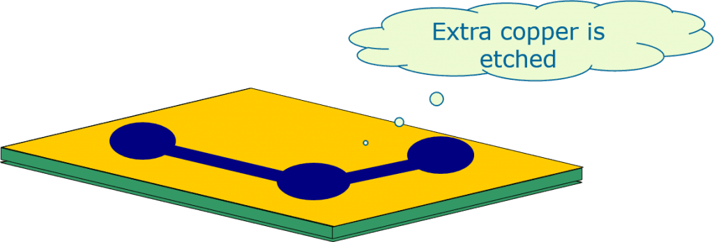
Inner-layer etching removes the unwanted copper exposed during developing. The hardened dry-film resist protects the circuit features that must remain, while the etchant dissolves the unprotected copper to define the inner-layer traces, pads, and copper planes.
Etchant chemistry, temperature, and processing speed are controlled to achieve the required conductor widths and clearances. Excessive etching can narrow traces through lateral undercut, while insufficient etching can leave residual copper between features. After etching, the panel is rinsed and proceeds to resist stripping.
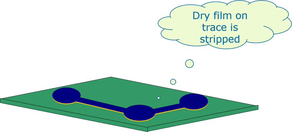
2.6. Inner-Layer Resist Stripping
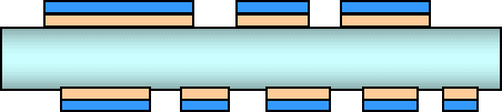
Inner-layer resist stripping removes the hardened dry film that protected the required copper features during etching. A suitable stripping solution breaks down and removes the remaining resist, exposing the etched copper circuitry without intentionally removing the circuit copper.
The panel is then thoroughly rinsed and checked for resist residues and surface contamination. The completed inner-layer pattern undergoes automated optical inspection (AOI) to check for defects such as opens, shorts, and deviations from the reference circuit data before bonding preparation and lay-up.

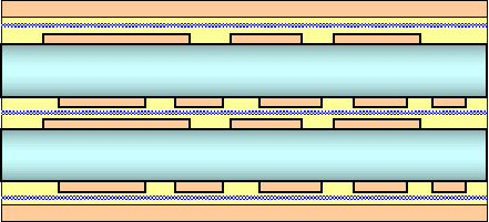
2.7. Multilayer PCB Lay-Up
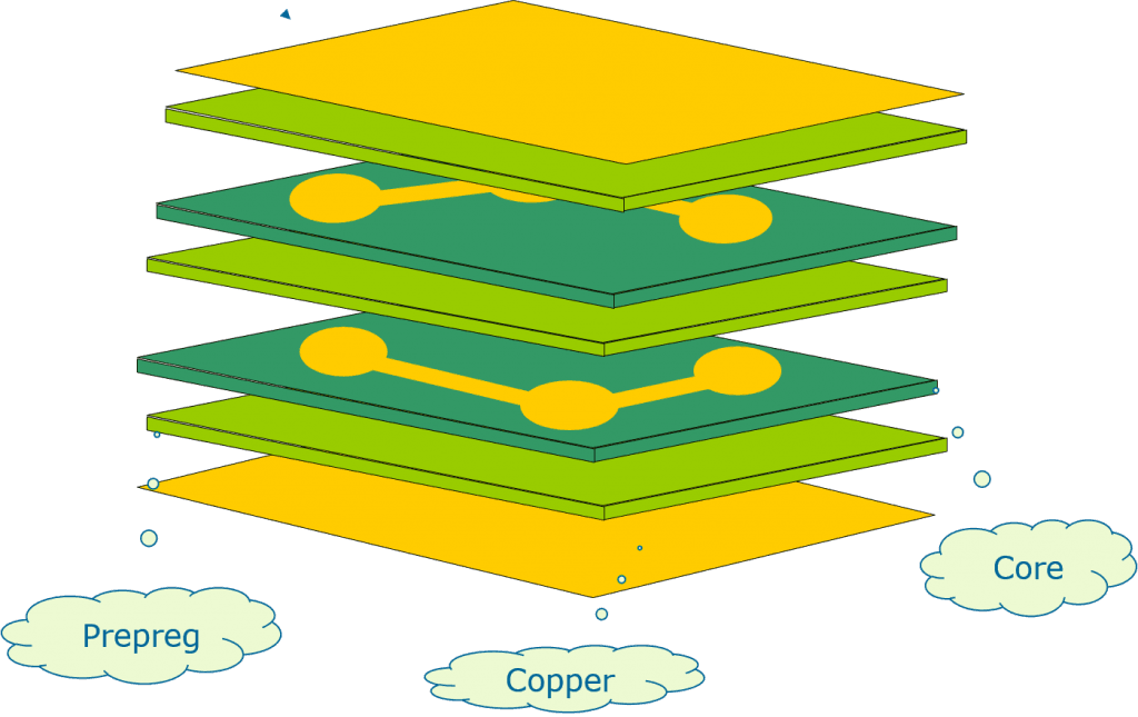
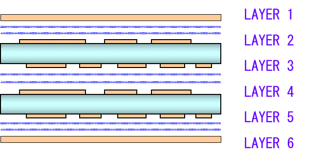
Multilayer PCB lay-up arranges the inspected inner-layer cores, prepreg, and outer copper foil in the sequence specified by the approved stack-up. Before assembly, the inner-layer copper surfaces receive a bonding treatment, such as an oxide or oxide-alternative process, to promote adhesion during lamination.
The layers are aligned using the production tooling and registration system. Layer order, core and prepreg thicknesses, copper weights, and material orientation are checked against the manufacturing instructions. Prepreg provides the insulating bonding material between the copper-clad cores and outer copper foil.
Lay-up produces an aligned stack ready for the lamination press; it does not complete the bonding process. In the next stage, controlled heat and pressure cause the prepreg resin to flow and cure, bonding the layers into a multilayer panel.
2.8. Multilayer PCB Lamination
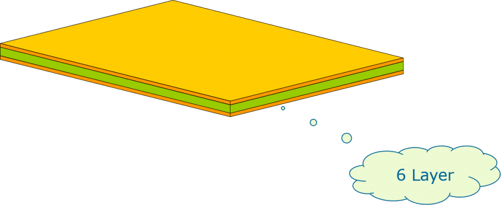
Multilayer PCB lamination bonds the prepared stack of inner-layer cores, prepreg, and outer copper foil into a single panel. During the press cycle, controlled heat causes the prepreg resin to soften and flow around the inner-layer copper features. Pressure consolidates the stack, and the resin then cures to form a solid insulating bond between the layers.
The heating rate, pressure, cure time, and cooling conditions are selected for the material system and panel construction. Proper control helps maintain the specified thickness, layer registration, and bonding integrity while reducing the risk of voids and delamination. After curing and controlled cooling, the laminated panel is ready for the subsequent drilling operations.
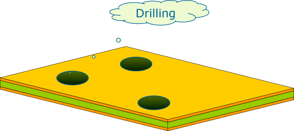
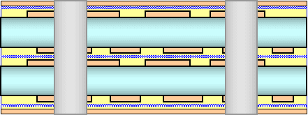
2.9. PCB Drilling
PCB drilling creates the holes required for plated through-hole connections, component leads, and mechanical mounting features. After lamination, panel registration is established so that the drilled holes align with the internal copper pads. X-ray registration may be used to locate inner-layer reference features and compensate for dimensional changes during lamination.
CNC drilling machines use production drill data derived from the approved NC drill files to control hole positions, tool sizes, and drilling sequences. Drill selection, spindle speed, feed rate, and tool condition are controlled to maintain hole accuracy and wall quality. Mechanical drilling is commonly used for through-holes, while laser drilling is typically used for microvias in HDI constructions.
After drilling, the panels undergo cleaning and hole preparation. Deburring removes raised material around the hole openings, while desmear removes resin residues that can cover the exposed inner-layer copper. These operations prepare the hole walls for reliable metallization in the next stage.
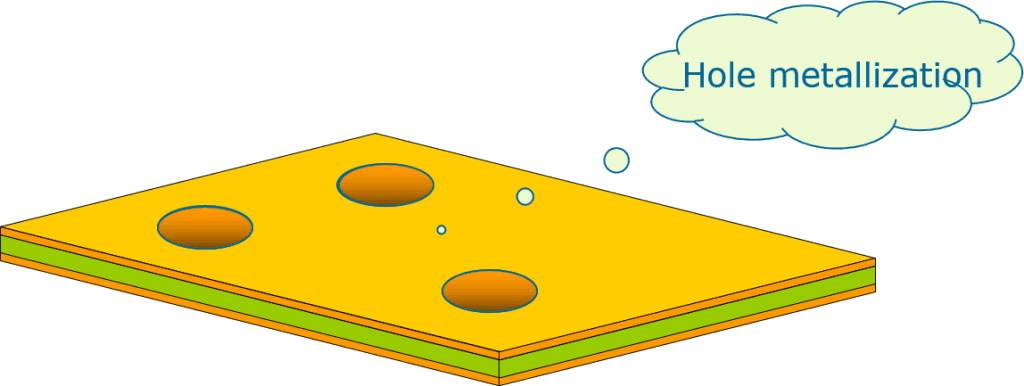
2.10. Through-Hole Metallization
Plated through-hole (PTH) processing makes the drilled hole walls conductive so that subsequent copper plating can establish electrical connections between layers. Because the exposed resin and glass reinforcement are non-conductive, the hole walls must first be cleaned, conditioned, and prepared for metallization.
In a conventional electroless copper process, the prepared surfaces are activated and a thin copper seed layer is chemically deposited on the hole walls and panel surfaces. This deposition does not require an external electrical current and provides the conductive base needed for subsequent electrolytic copper plating.
Copper is then built up through the specified panel-plating and/or pattern-plating stages to achieve the required finished hole-wall thickness. The initial electroless deposit alone is not the finished plated through-hole. Complete coverage, effective connection to the exposed inner-layer copper, and adequate final copper thickness are essential for reliable interlayer connections.
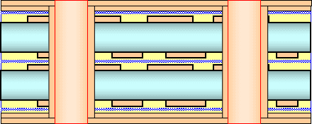
3. Multilayer PCB Outer-Layer Manufacturing Process
Outer-layer PCB manufacturing forms the external copper traces, pads, and planes after drilling and initial hole metallization. In the pattern-plating process described below, the main stages are dry-film application, exposure, developing, copper and tin plating, resist stripping, copper etching, and tin stripping.
The developed resist leaves openings over the required circuit features and plated through-holes. Additional copper is electroplated in these exposed areas, followed by a tin coating that serves as an etch resist. The dry film is then stripped, and the unwanted background copper is etched away. Finally, the tin is removed to reveal the completed outer-layer copper circuitry.
After circuit formation and inspection, solder mask is applied to protect selected areas while leaving the specified pads and other openings accessible. A surface finish protects exposed copper and prepares the solderable surfaces for assembly. The following sections explain each stage, from outer-layer image transfer through solder mask and surface finishing.

Outer-Layer Image Transfer Overview
Outer-layer image transfer defines where additional copper will be plated. A photosensitive dry film is applied to the prepared panel surfaces, exposed using the production artwork or direct imaging, and developed to create openings over the required traces, pads, and plated through-holes.
The key difference from the inner-layer process is the purpose of the resist pattern. During inner-layer etching, resist protects the copper that must remain. In the outer-layer pattern-plating process, resist covers the background areas while the required circuit features remain exposed for copper and tin plating. This distinction determines which areas are protected and which areas are processed in the following stages.
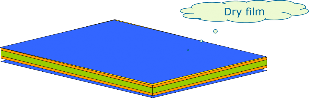
3.1. Outer-Layer Dry-Film Lamination
Outer-layer dry-film lamination applies a photosensitive plating resist to the prepared copper surfaces of the panel. Before application, the surfaces are cleaned and conditioned to remove oxidation and contamination that could affect adhesion. Controlled heat and pressure bond the dry film to the copper, creating a uniform coating for subsequent imaging.
In the pattern-plating process, this film acts as a temporary plating mask. After exposure and developing, it will cover the background areas while leaving the required circuit features accessible for copper and tin plating. Consistent adhesion and a surface free from wrinkles, trapped air, and particles help maintain well-defined plating boundaries.
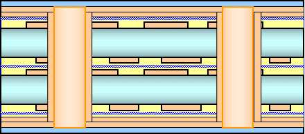
3.2. Outer-Layer Exposure
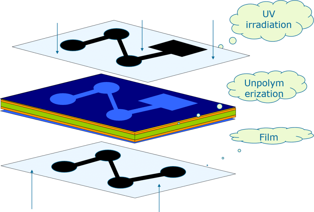
Outer-layer exposure transfers the production image onto the laminated dry-film resist. The image is aligned with the drilled panel so that the surface pads and circuit features register correctly with the plated through-holes. Exposure may use a phototool and UV light or direct imaging, depending on the production method.
For the negative-working dry film used in this pattern-plating process, the background areas are exposed and hardened, while the areas intended for copper and tin plating remain unexposed. Controlled image alignment and exposure help preserve the required pad positions, trace geometry, and plating openings for the developing stage.
3.3. Outer-Layer Developing
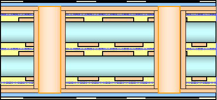
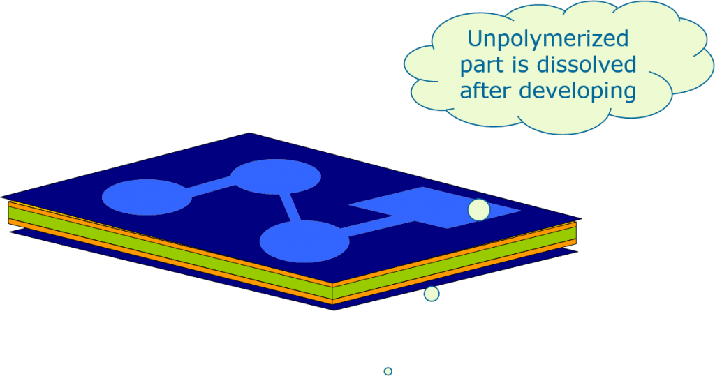
Outer-layer developing removes the unexposed dry film from the areas intended for pattern plating. The developer reveals the copper traces and pads to be built up and opens access to the plated through-holes, while the hardened resist remains over the background copper.
The panel is rinsed and checked for incomplete development, resist residues, and damage to the plating mask. Clean openings and well-adhered resist are important for keeping subsequent copper and tin deposition within the intended areas. At this stage, the background copper has not been etched away; the developed panel is ready for pattern plating.
3.4. Pattern Plating: Copper and Tin
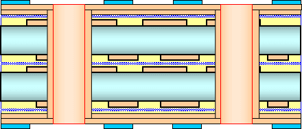
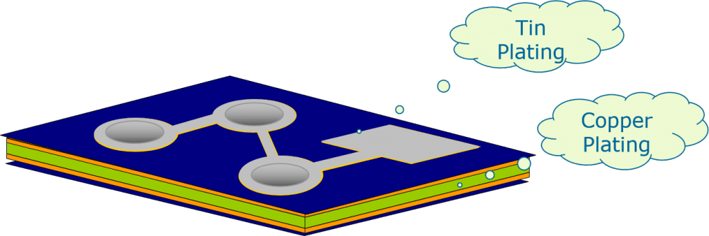
Pattern plating builds additional copper on the circuit features exposed during outer-layer developing, including traces, pads, and plated through-hole walls. The dry-film resist covers the background areas and prevents metal deposition there. Electrolytic copper plating increases the copper thickness in the exposed areas to meet the specified manufacturing requirements.
After copper plating, tin is electroplated over the exposed copper features. This tin layer serves as a temporary etch resist, protecting the required copper during subsequent outer-layer etching. Plating chemistry, current distribution, and processing time are controlled to achieve suitable copper coverage and a continuous tin coating.
3.5. Outer-Layer Resist Stripping
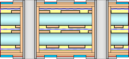
Outer-layer resist stripping removes the dry-film plating mask after copper and tin plating. The stripping solution removes the hardened resist from the background areas, exposing the underlying copper that must be etched away. The tin coating remains on the plated circuit features to protect them during the next stage.
Thorough stripping and rinsing help prevent resist residues from shielding unwanted copper during etching. At the end of this step, both the tin-covered circuit features and the exposed background copper are still present; the outer-layer circuit pattern has not yet been fully isolated.

3.6. Outer-Layer Copper Etching
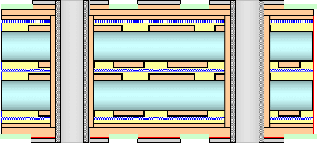
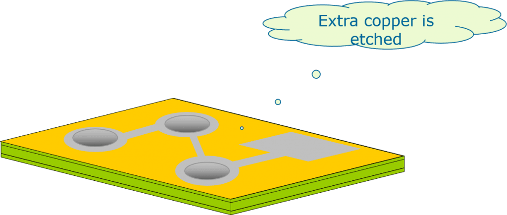
Outer-layer etching removes the background copper exposed after dry-film stripping. An etchant compatible with the tin etch resist dissolves the unwanted copper, while the tin coating protects the plated traces, pads, and through-hole connections. Removing the background copper electrically separates the required circuit features.
Etchant chemistry, temperature, and processing speed are controlled to clear the spaces between features while limiting lateral undercut. Incomplete etching can leave copper bridges that cause shorts, while excessive etching can reduce conductor widths. After etching and rinsing, the completed copper pattern remains covered by the temporary tin layer.
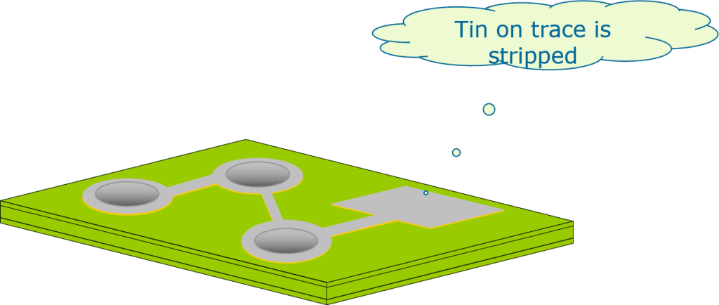
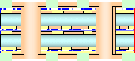
3.7. Tin Stripping
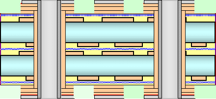
Tin stripping removes the temporary tin coating after outer-layer copper etching. A suitable stripping solution removes the tin while minimizing attack on the underlying copper, revealing the finished outer-layer traces, pads, and other circuit features.
The panel is then thoroughly rinsed and checked for residual tin, unwanted copper, and visible circuit defects. Outer-layer automated optical inspection (AOI) checks the circuit pattern against the reference data before solder mask processing. The copper surfaces are subsequently prepared for the next manufacturing stage.
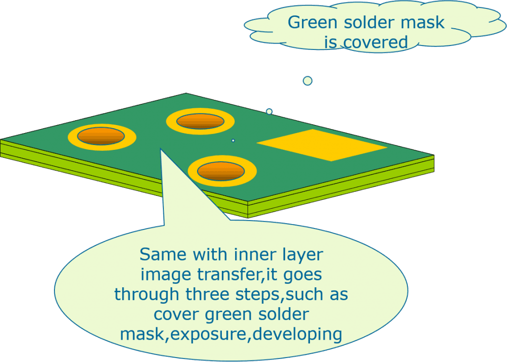
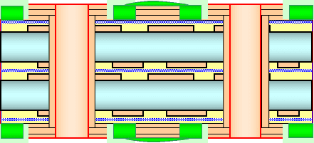
Solder mask is a protective polymer coating applied over selected areas of the PCB’s outer-layer circuitry. It helps protect the covered copper from contamination and unintended solder contact, while leaving openings for solderable pads, test points, and other features specified in the design. Where sufficient spacing is available, solder mask dams between adjacent pads help reduce the risk of solder bridging during assembly.
In a typical liquid photoimageable (LPI) solder mask process, the panel is cleaned, coated with solder mask ink, and dried to a suitable condition for imaging. The coating is then exposed using the solder mask artwork or direct imaging. Developing removes the unexposed material from the required openings, and a final cure gives the remaining coating its specified properties.
Inspection checks the mask’s alignment with the copper features, pad openings, coverage, adhesion, and visible defects such as pinholes or unwanted ink on pads. Accurate registration is particularly important around fine-pitch features, where misplaced mask can reduce the available soldering area or compromise the intended mask dams.
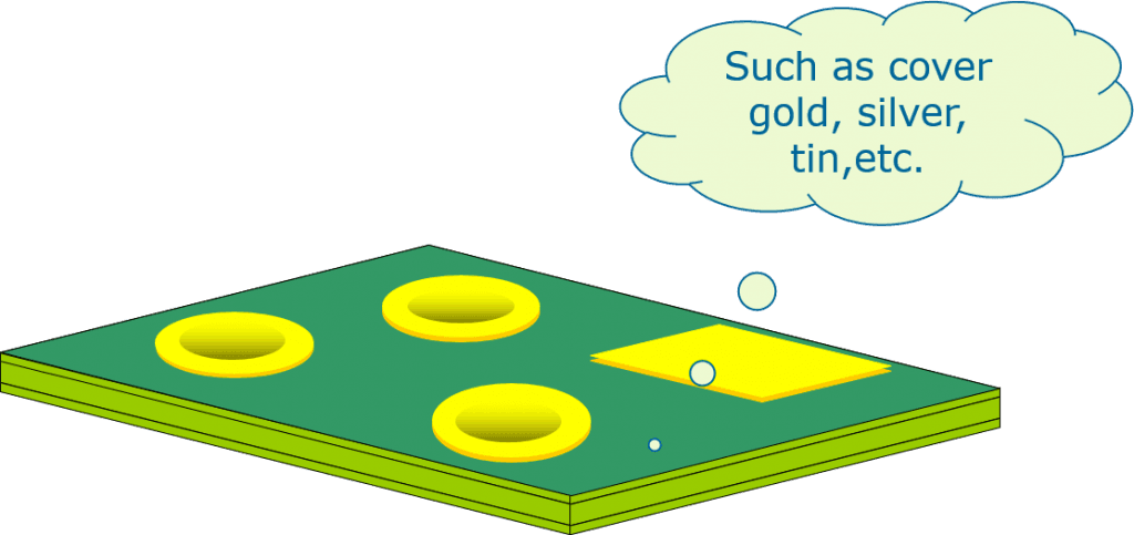
A PCB surface finish protects the exposed copper areas that are not covered by solder mask and preserves their solderability before assembly. Without suitable protection, copper can oxidize during handling and storage, making subsequent soldering more difficult. The finish is selected according to the board’s assembly requirements, pad geometry, storage conditions, and cost targets.
Common options include hot air solder leveling (HASL), lead-free HASL, electroless nickel immersion gold (ENIG), organic solderability preservative (OSP), immersion silver, and immersion tin. These finishes use different protection mechanisms: HASL leaves a leveled solder coating, ENIG forms a nickel layer with a thin protective gold layer, and OSP applies an organic protective film directly to the copper.
Selection involves trade-offs rather than a single best finish for every PCB. Pad flatness is important for fine-pitch assembly, while thermal exposure, handling sensitivity, and storage requirements also affect suitability. Finish coverage, cleanliness, and applicable coating thickness requirements are checked against the approved specification.
The surface finish applied here is distinct from the temporary tin etch resist used during outer-layer pattern plating. That earlier tin layer was removed after etching; this stage provides the specified finish on the completed board’s exposed copper features.
4. PCB Marking, Profiling, Testing, and Final Inspection
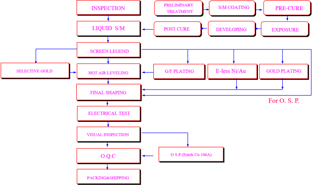
The final stages of PCB fabrication complete the board markings, define the finished outline, and verify that the bare boards meet the approved requirements. Depending on the manufacturing route, legend printing, surface finishing, and profiling may be arranged in different sequences.
Legend printing adds reference designators, polarity marks, logos, and other specified identification. Profiling forms the board outline using routing, V-scoring, punching, or a combination of methods suited to the design. Boards may remain in an agreed delivery panel rather than being separated into individual pieces.
Electrical testing checks continuity and isolation against the reference circuit data to identify opens and shorts. Final inspection checks the board’s appearance, dimensions, markings, solder mask, and surface finish against the applicable acceptance requirements. Accepted boards are then packaged to protect them during handling, storage, and shipment.
5, Summary
PCB fabrication turns approved design data into a finished bare circuit board through a controlled sequence of engineering, material preparation, circuit formation, layer bonding, hole metallization, and protective finishing. For a typical multilayer PCB, inner-layer circuits are formed and inspected before lamination, followed by drilling, outer-layer processing, solder mask, and surface finishing.
The exact manufacturing route depends on the board construction, materials, via structures, and specified requirements. The process described in this guide follows a conventional multilayer, plated through-hole construction with outer-layer pattern plating; HDI, sequential-lamination, and other specialized designs may require additional or repeated processing stages.
Before shipment, electrical testing and final inspection check the completed bare boards against the approved production data and applicable acceptance requirements. Clear fabrication files, an agreed stack-up, and well-defined material, copper, finish, and tolerance requirements help establish a consistent basis for manufacturing and inspection.
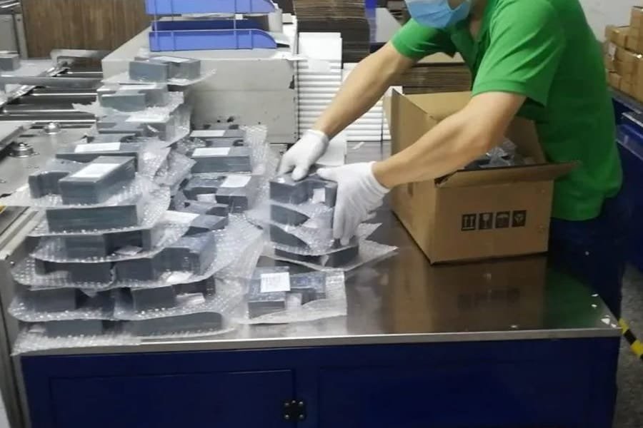
A super detailed step-by-step guide to the PCB manufacturing process


Why Understanding the PCB Fabrication Process Matters
Understanding PCB fabrication helps designers and buyers connect board requirements with manufacturing decisions. It provides a practical basis for reviewing manufacturability, evaluating cost trade-offs, and specifying appropriate quality checks.
Design for Manufacturability
Review trace spacing, hole sizes, annular rings, copper distribution, and board-edge clearances with fabrication in mind. Identifying manufacturing constraints early helps resolve design issues before production begins.
Cost and Lead-Time Planning
Layer count, materials, via structures, tolerances, and surface finishes influence the manufacturing route. Understanding these choices helps you discuss cost and lead-time trade-offs without overlooking essential performance requirements.
Quality and Reliability
Knowing where imaging, lamination, plating, and inspection occur helps you define relevant acceptance requirements. It also supports clearer discussions about electrical testing, dimensional checks, and manufacturing documentation.
FAQs About the PCB Fabrication Process
PCB fabrication produces the bare circuit board, including its copper circuits, insulating layers, holes, solder mask, and surface finish. PCB assembly is a separate process that mounts and solders electronic components onto that board. This guide covers bare PCB fabrication, not component assembly.
Multilayer PCB fabrication includes forming and inspecting internal copper circuits, then bonding the inner-layer cores with prepreg and outer copper foil. Double-sided PCBs do not require this inner-layer lay-up and multilayer lamination stage. Both constructions can use plated through-holes to connect copper layers.
Both processes transfer circuit information onto photoresist, but the resist serves different purposes in the manufacturing route described here. Inner-layer resist protects the copper that must remain during etching. In outer-layer pattern plating, resist covers the background while the required circuit features remain open for copper and tin plating.
Plated holes provide electrical connections between copper layers and can also accommodate through-hole component leads. After drilling and hole preparation, metallization makes the non-conductive hole walls conductive, and subsequent copper plating builds the required copper thickness. Mechanical mounting holes may be specified as non-plated when no electrical connection is needed.
No. Dry-film lamination applies a photosensitive resist to copper surfaces for circuit imaging. Multilayer PCB lamination bonds inner-layer cores, prepreg, and outer copper foil into a single panel using controlled heat and pressure. They are separate operations with different materials and purposes.
Electrical testing checks continuity and isolation against the reference circuit data to identify opens and shorts. Final inspection checks features such as board dimensions, markings, solder mask, surface finish, and visible workmanship. Additional checks depend on the board specification and agreed acceptance requirements; electrical testing alone does not verify every aspect of reliability.
No. The manufacturing route depends on layer count, materials, via structures, copper requirements, and other design features. This guide describes a conventional multilayer plated through-hole process with outer-layer pattern plating. HDI boards, blind or buried vias, and sequential-lamination constructions may require additional or repeated processing stages.
A typical fabrication package includes Gerber files or another agreed manufacturing data format, NC drill files, a board outline, and fabrication notes. Multilayer boards also need a defined or agreed stack-up. Specify materials, finished thickness, copper requirements, surface finish, tolerances, and any controlled-impedance requirements so the manufacturer can review the job before production.
Ready to Discuss Your PCB Fabrication Requirements?
Send PCBELEC your Gerber files, NC drill files, and fabrication requirements to request a bare PCB manufacturing quotation. Include your required quantity, layer count, finished thickness, copper requirements, and surface finish, together with any stack-up, controlled-impedance, or special tolerance requirements.
Request a PCB Fabrication QuoteHave a target delivery date or an unresolved stack-up requirement? Include it with your inquiry for review.