Double-Sided Flex PCB Manufacturing Services

Custom 2-Layer Flexible Circuits and Double-Sided Flex PCBs from a China Manufacturer

JHYPCB specializes in reliable double-sided flex PCB manufacturing for customers worldwide. Our 2-layer flexible circuits are ideal for space-constrained, high-density designs in consumer electronics, automotive, medical, industrial control, and other demanding applications. Get engineering-driven support from prototype to small and medium-volume production.

  • Double-sided flex PCB and 2-layer flexible PCB manufacturing services.
  • IPC-compliant fabrication with multiple copper thicknesses and PI-based materials.
  • Quick-turn double-sided flex PCB prototypes and small-batch production runs.
  • Stiffeners, coverlay, and assembly options for complex flexible circuit designs.
  • 100% electrical testing and AOI inspection for every flex PCB.

What Is a Double-Sided Flex PCB?

A double-sided flex PCB, also called a double-sided flexible PCB or 2-layer flexible PCB, is a flexible printed circuit with two copper conductor layers on a bendable base film. Both sides of the polyimide core carry etched copper traces, and plated through holes connect the top and bottom layers to create more complex circuits than single-sided flex designs. According to IPC 6013, this structure is classified as a Type 2 double-sided flex circuit.

Compared with single-sided flex PCBs, double-sided flex PCBs offer higher routing density and more design freedom in the same or even smaller area. This makes double-sided flexible circuits a popular choice for space-constrained applications such as consumer electronics, automotive electronics, medical devices, industrial control, and other high-density interconnects that still require excellent flexibility and lightweight construction.

what is double sided flexible PCB

Typical 2-Layer Flexible PCB Stackup

A standard double-sided flex PCB stackup places two copper layers around a thin flexible core, with protective coverlay on both sides, to balance flexibility, durability, and electrical performance.

Layer (Top to Bottom)Description
Top CoverlayPolyimide coverlay with openings for pads and flex areas
Top Copper LayerEtched copper traces on the top side of the flexible core
Flexible Core (PI)Thin polyimide base film providing flexibility and insulation
Bottom Copper LayerEtched copper traces on the bottom side of the core
Bottom CoverlayPolyimide coverlay protecting circuits on the bottom side

By adjusting the copper thickness, polyimide thickness, adhesives, and coverlay construction, double-sided flexible PCBs can be optimized for different bend requirements, current levels, and reliability targets in your design.

Special possibilities

a)Different stiffener thicknes from each side are alowed
b)Also more sitiffener thickness from one side is alowed
c)Double sided tape on flex or stiffener for sticking PCB to final product

Double-Sided Flex PCB Stackup & Materials

A double-sided flex PCB stackup combines two copper layers, a flexible dielectric core, protective coverlay, and optional stiffeners to achieve the right balance of flexibility, reliability, and assembly robustness. By carefully selecting materials and layer constructions, JHYPCB can optimize your double-sided flexible PCB for bending performance, thermal stability, and electrical requirements.

Standard 2-Layer Double-Sided Flex PCB Stackup

A typical 2-layer flexible PCB stackup for double-sided flex circuits includes two copper foil layers on a polyimide core, insulated and protected by coverlay films.

Layer (Top → Bottom)Description
Top CoverlayPolyimide coverlay or flexible solder mask protecting the top copper traces while leaving pads and flex areas exposed as required.
Top Copper LayerEtched copper foil forming the top-side circuitry of the double-sided flex PCB.
Flexible Core (Polyimide)Thin polyimide base film providing electrical insulation, flexibility, and thermal stability for the 2-layer flexible PCB stackup.
Bottom Copper LayerEtched copper foil forming the bottom-side circuitry, interconnected with the top layer through plated through holes.
Bottom CoverlayPolyimide coverlay or flexible solder mask protecting the bottom copper and improving mechanical and chemical resistance.

Depending on your double-sided flex PCB design, we can adjust copper weight, core thickness, adhesive systems, and coverlay constructions to support dynamic bending zones, controlled impedance, and specific assembly processes.

Base Materials for Double-Sided Flexible PCBs

For most double-sided flex PCB projects, JHYPCB uses polyimide (PI) as the primary flexible base material because it offers excellent thermal stability, mechanical strength, and flexibility over a wide temperature range. Polyester (PET) and polyethylene naphthalate (PEN) can be considered for cost-sensitive or less demanding environments, while advanced materials such as liquid crystal polymer (LCP) may be used when low loss and high-frequency performance are critical.

  • Standard base: polyimide film for most double-sided flexible PCB applications.
  • Optional PET or PEN for lower-temperature, cost-conscious designs.
  • LCP and other specialty materials available for high-frequency or low-loss requirements.

Copper Thickness, Coverlay, and Surface Finishes

The copper layers in a 2-layer flexible PCB can be manufactured with different copper weights depending on current and bend requirements, typically ranging from very thin foils for dynamic flex to heavier copper for power traces. Rolled annealed (RA) copper is often preferred for double-sided flex PCBs that will experience repeated bending, while electro-deposited (ED) copper may be suitable for more static applications. Coverlay films or flexible solder masks are then applied to protect the traces and define solderable pad areas.

To support different assembly processes, JHYPCB offers a range of surface finishes for double-sided flex PCBs, including:

  • ENIG (electroless nickel immersion gold) for fine-pitch and high-reliability applications.
  • Immersion tin and immersion silver for cost-effective solderability.
  • ENEPIG for mixed-technology assemblies and wire bonding requirements.
  • OSP and other specialized finishes on request.

Stiffeners and Mechanical Support for Double-Sided Flex PCBs

Many double-sided flexible PCB designs require local mechanical reinforcement in connector, component, or solder joint areas. To meet these needs, JHYPCB can integrate different types of stiffeners into your double-sided flex PCB stackup so that you maintain flexibility where it is needed while achieving the required rigidity and thickness in critical zones.

  • Polyimide stiffeners for controlled thickness in ZIF connector fingers and support around fine-pitch components.
  • FR-4 stiffeners for robust support in connector areas and around heavy components.
  • Stainless steel or aluminum stiffeners for high-strength, high-heat, or mechanically demanding applications.

By combining the right double-sided flex PCB materials, copper construction, coverlay system, and stiffener options, our engineers can help you achieve a reliable and manufacturable 2-layer flexible PCB solution that matches your mechanical and electrical design goals.

Double sided Flexible PCB material

Benefits of Double-Sided Flex PCBs

Double-sided flex PCBs combine the mechanical advantages of flexible circuits with the higher circuit density and design freedom of double-sided boards. By routing traces on both sides of a flexible substrate and interconnecting them through vias, double-sided flexible PCBs enable more compact, reliable, and lightweight electronic assemblies than many traditional rigid or single-sided flex solutions.

double sided flex pcb key advantages

Key Advantages in Your Designs

  • Higher circuit density in limited space – Conductive layers on both sides of the flexible base allow you to place more traces and components in the same footprint, which is critical for miniaturized electronics.
  • Improved design flexibility and routing freedom – Being able to route signals on both sides of the flex PCB makes it easier to implement complex interconnects, separate sensitive signals, and optimize power and ground paths.
  • Space and weight reduction – Double-sided flexible PCBs can replace multiple rigid boards, connectors, and wire harnesses, reducing overall weight and saving valuable space in compact enclosures.
  • Fewer connectors and interconnects – Integrating wiring into the double-sided flex PCB reduces the number of separate cables and plug-in connectors, which simplifies assembly and lowers potential failure points.
  • Enhanced reliability under mechanical stress – Properly designed double-sided flexible PCBs can withstand repeated bending, vibration, and thermal cycling better than many rigid interconnect solutions, especially in dynamic applications.

Compared with Single-Sided and Multilayer Flex PCBs

When you compare double-sided flex PCBs with single-sided and multilayer flex designs, they often provide a balanced choice between cost, complexity, and performance for many medium-density applications.

  • More routing capability than single-sided flex PCBs – Double-sided flexible circuits overcome the routing limitations of single-sided flex by adding a second copper layer and vias, enabling more complex circuits without significantly increasing board size.
  • Smaller and cleaner layouts – With traces on both sides, you can reduce or eliminate jumper wires and crossovers that are often needed on single-sided designs, resulting in cleaner layouts and easier assembly.
  • Lower cost and simpler fabrication than multilayer flex PCBs – Compared with multilayer flexible circuits, double-sided flex PCBs usually have fewer layers, less complex lamination, and shorter lead times, which can reduce overall manufacturing costs.
  • Good compromise between performance and manufacturability – For many projects, double-sided flexible PCBs provide enough routing density and signal performance without the complexity of full multilayer flex, making them a practical choice for medium- to high-density designs.
Comparison of single-sided, double-sided and multilayer flex PCBs illustrating different routing density, layer count and design complexity

Thanks to this combination of compact size, flexibility, and robust electrical performance, double-sided flex PCBs are widely used in consumer electronics, automotive systems, medical devices, industrial control, aerospace, and many other advanced applications.

Applications of Double-Sided Flex PCBs

Double-sided flex PCBs are widely used wherever compact size, lightweight construction, and reliable interconnection are required in a mechanically constrained environment. By placing circuitry on both sides of a flexible substrate, double-sided flexible PCBs support more complex functions in smaller spaces across consumer electronics, automotive, medical, industrial, and other advanced applications.

Wearable devices and consumer electronics using double-sided flex PCBs in smartwatches, fitness trackers and wireless earbuds
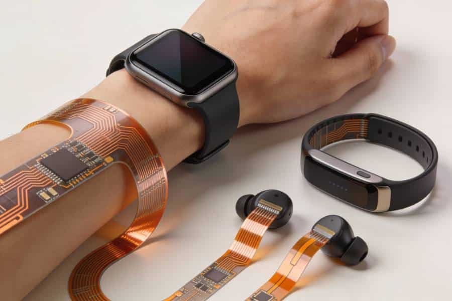
Wearable Devices & Consumer Electronics
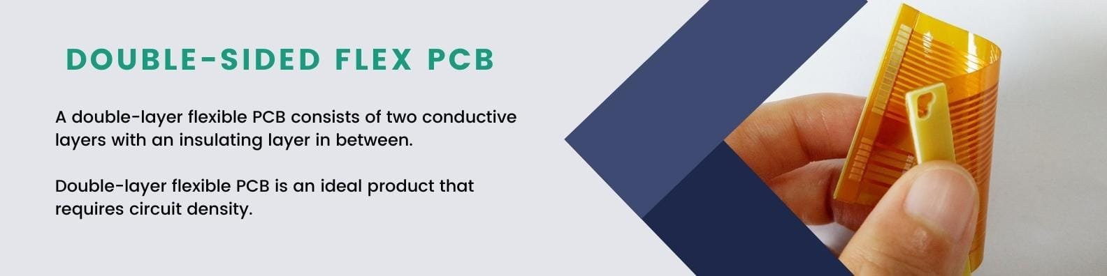
Double-sided flexible PCBs are ideal for wearable devices and consumer electronics that must fit into thin, curved housings, such as smartwatches, fitness trackers, wireless earbuds, foldable phones, and compact cameras. The ability to route signals on both sides of the flex circuit enables higher component density and cleaner layouts in very limited space.
double sided flex pcb automotive electronics lighting
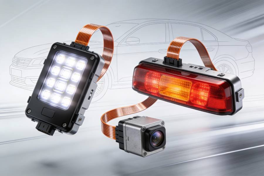
Automotive Electronics & Lighting Systems
In automotive electronics, double-sided flex PCBs are used in instrument clusters, infotainment systems, LED lighting modules, sensors, and control units where vibration, temperature cycling, and tight packaging are common. Flexible double-sided PCBs help reduce wiring harnesses, simplify connections between modules, and support creative 3D routing inside dashboards and lighting assemblies.
Medical devices and healthcare equipment using double-sided flex PCBs in patient monitors, diagnostic probes and wearable health sensors
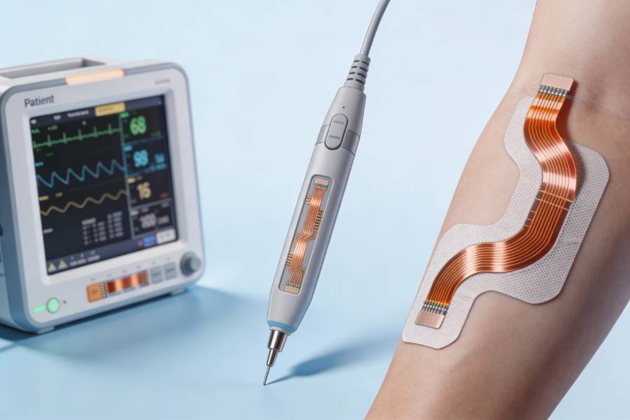
Medical Devices & Healthcare Equipment
Medical devices such as patient monitors, diagnostic probes, imaging equipment, and wearable health sensors use double-sided flex PCBs to achieve thin, lightweight, and ergonomically shaped electronics that can conform to the human body or fit into miniature housings. The combination of flexibility and higher circuit density allows more sensing, processing, and communication functions in compact medical and healthcare systems.
Industrial control systems and robotics using double-sided flex PCBs in robotic arms, sensors and compact control modules
Industrial Control & Robotics
In industrial control systems and robotics, double-sided flexible PCBs enable reliable connections in moving joints, articulated robot arms, sensors, and compact control modules. Using double-sided flex circuits instead of separate cables and connectors reduces mechanical stress on solder joints, improves reliability in dynamic motion, and simplifies assembly in tight industrial enclosures.
Aerospace, defense and other high-reliability systems using double-sided flex PCBs in avionics, satellite modules and communication equipment
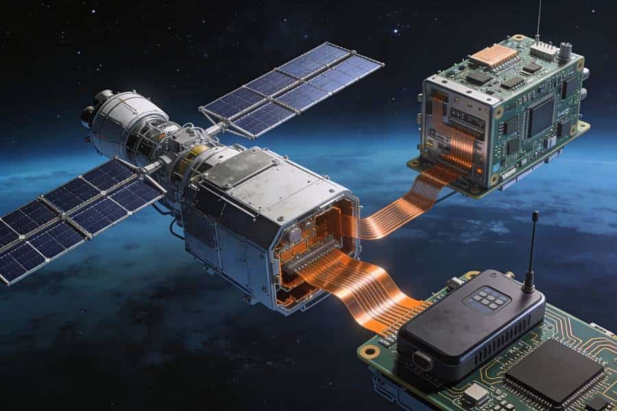
Aerospace, Defense & High-Reliability Systems
Aerospace and defense applications benefit from double-sided flex PCBs because they combine high circuit density with low weight and excellent resistance to vibration and mechanical shock. These flexible circuits can be used in avionics modules, satellite subsystems, communication equipment, and other mission-critical electronics where space and weight are tightly constrained.
High-density interconnects and board-to-board links using double-sided flex PCBs to connect rigid PCBs with folded flexible circuits
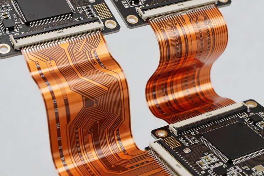
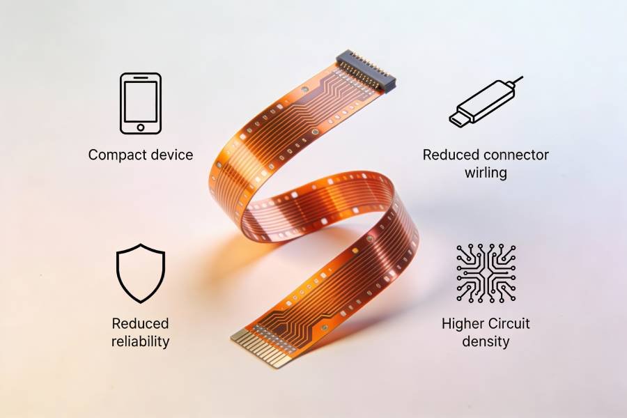
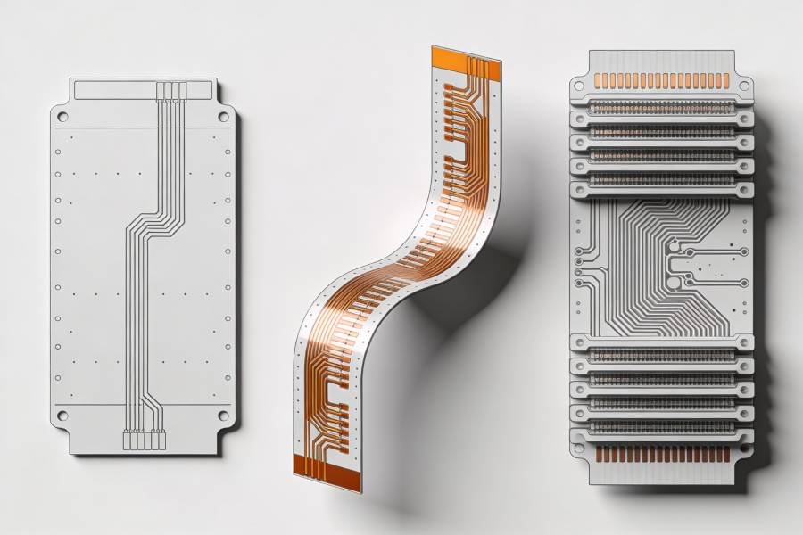
High-Density Interconnects & Board-to-Board Links
Double-sided flex PCBs are also used as high-density interconnects and board-to-board links in complex electronic assemblies. They can replace multiple connectors and ribbon cables by integrating routing into a single 2-layer flexible PCB, which improves signal integrity, reduces connection count, and allows creative folding or bending paths between rigid boards and modules.

Single-Sided, Double-Sided and Multilayer Flex PCBs – How to Choose

Flexible circuits are commonly available as single-sided, double-sided, and multilayer flex PCBs, each offering different levels of routing density, cost, and mechanical performance. Understanding the strengths and limitations of each type helps you choose the most appropriate flexible PCB construction for your application.

Overview: Comparing Flex PCB Types

Flex PCB TypeStructure & LayersTypical Use CasesMain AdvantagesMain Limitations
Single-Sided Flex PCBOne copper layer on a flexible substrate with coverlay on one side.Simple, low‑density circuits; jumpers; basic interconnects in low to medium complexity products.Lowest cost and simplest construction, excellent flexibility, easy to manufacture and assemble.Limited routing capacity, no vias between layers, not suitable for high‑density or complex designs.
Double-Sided Flex PCBTwo copper layers on a flexible substrate with vias connecting top and bottom layers.Medium‑density circuits that need more routing and components in compact spaces.Higher circuit density than single‑sided flex, better routing freedom, good balance between performance and cost.Slightly higher cost and complexity than single‑sided; somewhat reduced flexibility compared with single‑layer constructions.
Multilayer Flex PCBThree or more flexible copper layers laminated together, often with rigid sections in rigid‑flex designs.High‑density, complex, high‑reliability systems such as advanced medical, aerospace, and communication equipment.Maximum routing density, supports complex impedance‑controlled and high‑speed designs, can integrate multiple functions in one flex assembly.Highest cost and manufacturing complexity, reduced overall flexibility, longer lead times and tighter design rules.

How to Select the Right Flex PCB Type

  • Circuit complexity and routing density – If your design is simple and low‑density, a single‑sided flex PCB is usually sufficient. When you need more routing channels and component density in a limited area, a double-sided flex PCB is often the best compromise before moving to multilayer flex.
  • Available space and mechanical constraints – For extremely tight spaces and simple functions, single‑sided flex circuits offer maximum bendability. When you need more functions in the same or smaller footprint, double-sided flexible PCBs allow denser layouts without adding rigid boards or connectors.
  • Flexibility and bend requirements – Single‑sided flex PCBs generally provide the highest dynamic flex life, while double-sided flex PCBs maintain good flexibility with higher routing capability. Multilayer flex designs trade some flexibility for density and are more suitable for limited bending or mostly static flex regions.
  • Budget and manufacturing complexity – Single‑sided flex circuits are the most economical and easiest to fabricate, double-sided flex PCBs add moderate cost and complexity, and multilayer flex circuits are the most expensive and demanding in terms of process control and design rules.
  • Reliability and performance targets – When you require high‑reliability interconnects with moderate complexity, double-sided flex PCBs usually offer a good balance between performance and manufacturability. If your design demands very high I/O counts, advanced high‑speed interfaces, or integration of multiple rigid areas, multilayer flex or rigid‑flex may be the right choice.

If you are unsure whether a single-sided, double-sided, or multilayer flex PCB is best for your project, the engineering team at JHYPCB can review your requirements and recommend an optimized flexible PCB construction that balances performance, flexibility, and cost.

Our Double-Sided Flex PCB Manufacturing Capabilities

JHYPCB provides complete double-sided flex PCB manufacturing services, from engineering review and stackup design through fabrication, testing, and optional assembly. Our capabilities cover a wide range of 2-layer flexible PCB constructions, materials, and surface finishes to support both prototypes and volume production.

Core Manufacturing Capabilities

CapabilityTypical Range / Options
Board type2-layer double-sided flex PCBs (IPC 6013 Type 2)
Base materialsPolyimide (standard), PET / PEN / specialty films on request
Copper thicknessTypically 0.5 oz–2 oz (other weights available on request)
Min trace / spacee.g. 3/3 mil or 4/4 mil depending on stackup and material set
Finished flex thicknessConfigurable based on copper and core thickness for your design
Coverlay / solder maskPolyimide coverlay, photo‑imageable coverlay, flexible solder mask
StiffenersPolyimide, FR‑4, stainless steel, aluminum in selected areas
Surface finishesENIG, immersion tin, immersion silver, ENEPIG, OSP and others
Drill / viaPlated through holes for double‑sided interconnection, via sizes per design rules
Testing100% electrical test, AOI, and other inspections as required

Our engineering team can help you choose suitable materials, copper weights, and stiffener options for your double-sided flex PCB so that your design meets mechanical, thermal, and electrical requirements while remaining manufacturable and cost-effective.

How to Order Double-Sided Flex PCBs from JHYPCB

Ordering double-sided flex PCBs from JHYPCB is straightforward. Follow the simple steps below to share your design files and requirements so that our engineers can review your project and provide a fast, accurate quotation.

To achieve the best results and the most competitive pricing for your double-sided flex PCBs, please share any special reliability, bend radius, or assembly requirements with us in advance so our team can optimize materials, stackup, and panelization for your project.

Double-Sided Flex PCB FAQ

A double-sided flex PCB, also called a double-sided flexible PCB or 2-layer flexible PCB, is a flexible printed circuit with copper circuitry on both sides of a bendable base material such as polyimide. The two copper layers are interconnected by plated through holes, which allows more complex routing and higher circuit density than a single-sided flex design.

You typically choose a double-sided flex PCB when a single-sided flex circuit does not provide enough routing density or design flexibility for your application. If you need more traces, additional components, or better separation of signals and power in a compact area, a double-sided flexible PCB offers a good balance between complexity, cost, and performance.

The thickness of a double-sided flex PCB depends on the chosen copper weights, core thickness, adhesives, and coverlay, but many 2-layer flexible PCB stackups are designed to be very thin compared with rigid boards. Thinner constructions are often used in dynamic flex areas, while slightly thicker constructions with stiffeners can be used in connector or component regions to improve mechanical stability.

Most double-sided flex PCBs use polyimide film as the flexible base material because it offers excellent thermal stability, mechanical strength, and flexibility. Copper foils form the conductive layers, while coverlay films or flexible solder masks provide insulation and environmental protection. Depending on the application, polyester, PEN, LCP, and different adhesive systems may also be used.

The recommended minimum bend radius for a double-sided flex PCB depends on total thickness, copper type, and whether the bend is static or dynamic. In general, double-sided flex circuits require a larger bend radius than single-sided flex circuits, and it is important to follow manufacturer bend radius guidelines to avoid copper cracking or delamination in repeated bending applications.

Yes, components can be mounted on double-sided flex PCBs, but it is usually recommended to use stiffeners under component and connector areas to support the solder joints and control local thickness. Stiffeners help prevent stress on solder joints when the surrounding flex region bends and improve handling during assembly.

Common surface finishes for double-sided flexible PCBs include ENIG, immersion tin, immersion silver, ENEPIG, and OSP. The best choice depends on your component types, assembly process, and reliability requirements, with ENIG and ENEPIG often preferred for fine-pitch or high-reliability applications.

JHYPCB can support double-sided flex PCB prototypes as well as small and medium production runs, allowing you to validate your design before moving to higher volumes. By sharing your target quantity and schedule, we can recommend appropriate panelization, stackup, and cost-optimized options for your project.

To provide an accurate quotation for a double-sided flex PCB, we typically need your Gerber or ODB++ files, layer stackup or key thickness information, base material, copper weight, surface finish, stiffener requirements, expected quantity, and any special reliability or bend requirements. The more complete your information, the faster we can review your design and return a competitive quote.

Yes, JHYPCB offers engineering support for double-sided flex PCB design, including stackup recommendations, material selection, bend area optimization, and design-for-manufacturability reviews. Sharing your drawings, bend diagrams, and key performance requirements early in the process allows us to help you avoid common flex PCB design mistakes and improve long-term reliability.

Ready to Start Your
Double-Sided Flex PCB Project?

If you are planning a new design that requires reliable double-sided flex PCBs or 2-layer flexible circuits, JHYPCB is ready to support you from concept and prototyping through to production. Our team can help you refine your stackup, select suitable materials and stiffeners, and optimize your design for manufacturability and long-term reliability.

Share your files and requirements with us today to receive a fast, detailed quotation for your double-sided flex PCB project, along with engineering feedback where needed. Whether you need a few prototypes or ongoing production, we will work with you to deliver high-quality flexible PCBs on time and within budget.

Related Reading

Scroll to Top