Gold Finger PCB Fabrication & Manufacturing Service
Hard gold finger edge connectors with 3–50 µin plating, 30°–45° bevel, IPC‑compliant quality, and fast prototype or small‑batch production for your most demanding PCB gold fingers and edge connector applications.
- Hard gold or ENIG options to match your required mating cycles
- Typical gold thickness from 3–50 µin and 30°–45° bevel angle for smooth insertion
- Flexible capabilities from simple 2-layer boards to complex multilayer designs
- One-stop service: engineering support, DFM check, fabrication and assembly in China
Typical response time within 24 hours for RFQs and DFM feedback.
Gold Finger PCB Guide – Quick Navigation
6 Layer Gold Fingers PCB
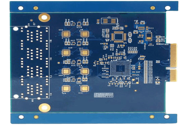
Double Layer Gold Fingers PCB
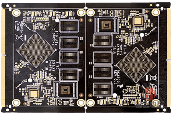
Double-sided Gold Fingers PCB
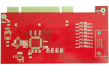
Double Layer Gold Fingers PCB
What is a Gold Finger PCB?
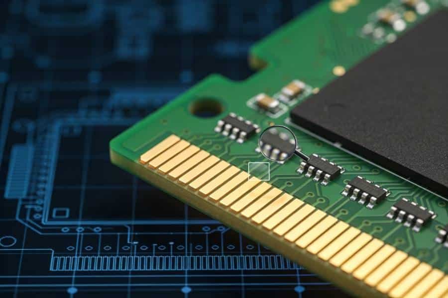
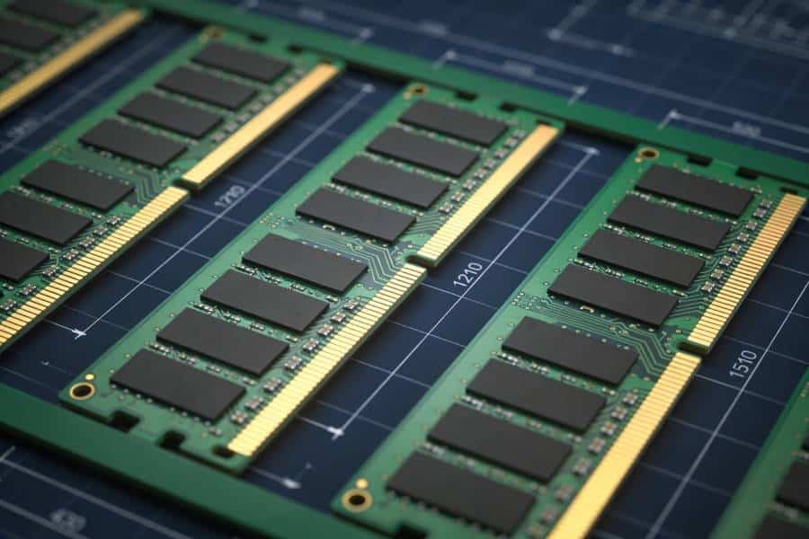
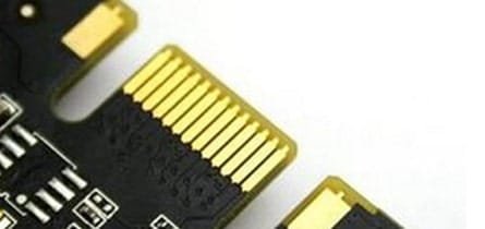
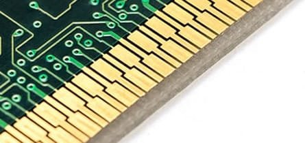
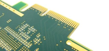
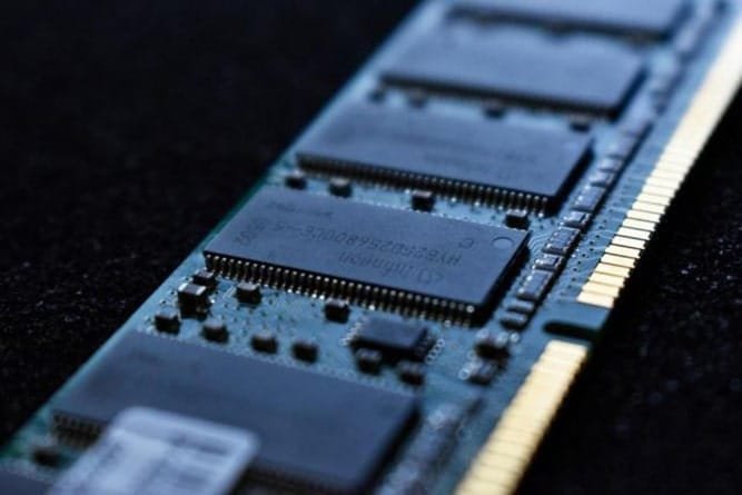
Gold fingers are the gold‑plated edge connectors you see along the side of many PCBs, such as memory cards, graphics cards, SSDs and various expansion boards. These flat, exposed pads form a plug‑in interface that allows the PCB to slide directly into a mating connector or slot on a larger board, without using cables.
In a gold finger PCB, the copper pads at the board edge are covered with a hard gold or ENIG surface finish to provide low contact resistance and excellent resistance to oxidation and wear. The fingers are typically beveled at 30°–45° so that the board can be inserted smoothly and make reliable contact even after many mating cycles.
By arranging multiple fingers in a precise pattern and spacing, designers can route separate power rails, high‑speed signals and control lines through a single compact edge connector. This makes gold finger PCBs ideal wherever you need detachable modules, easy upgrades or high‑density connections between a main board and daughter cards. For this reason, many projects benefit from using a dedicated gold finger PCB fabrication service instead of a generic PCB process.
Gold Finger PCB Design Guidelines
When you design a gold finger PCB, a few critical geometry and layout rules will directly affect reliability, contact resistance and long‑term wear performance. The edge connector pads, bevel angle, spacing, surface finish and keep‑out areas must all be defined clearly so that fabrication and assembly can follow the same expectations.
At JHYPCB, we follow typical industry practices based on IPC guidelines and our manufacturing partners’ capabilities, while still being able to customize the exact values for your project when needed. The table below summarizes common design recommendations for gold finger PCBs and can be used as a starting point during schematic and layout.
| Design parameter | Typical recommendation | Notes |
|---|---|---|
| Gold type | Hard gold (electroplated) or ENIG | Hard gold for frequent mating cycles; ENIG for prototypes or low wear. |
| Gold thickness on fingers | 3–50 µin hard gold | Thicker plating for higher mating cycles and harsh environments. |
| Bevel angle | 30°–45° | Beveled edge makes insertion smoother and protects the pads. |
| Bevel length | 0.3–0.8 mm (typical) | Exact value depends on board thickness and connector type. |
| Finger width | Defined by connector, often 0.8–1.5 mm | Match the mating connector footprint and current requirement. |
| Finger spacing (pitch) | Defined by connector, often 1.0–1.27 mm | Keep consistent pitch for reliable engagement. |
| Copper under fingers | Full copper pads with nickel underlayer | Nickel acts as a barrier and supports the hard gold layer. |
| Solder mask | No solder mask on the gold finger pads | Keep mask clearance so the contact area stays completely exposed. |
| Silkscreen | No silkscreen over fingers or bevel | Avoid any ink on the contact surface. |
| Vias near fingers | No vias in pads; keep vias at least 0.5–1.0 mm away from fingers | Prevent plating leakage and mechanical weakness. |
| Board thickness at edge | Commonly 1.0–2.0 mm (0.8–3.2 mm available on request) | Must match the connector slot thickness. |
| Surface finish on the rest of PCB | ENIG / HASL / OSP, as needed | Fingers can use hard gold while other pads use a different finish. |
These values are typical and can be adjusted to match your specific connector, board thickness and mating cycle requirements. If you share your connector datasheet or mechanical drawing with us, our engineers can review the gold finger layout and suggest the optimal bevel angle, plating thickness and keep‑out distances before fabrication.
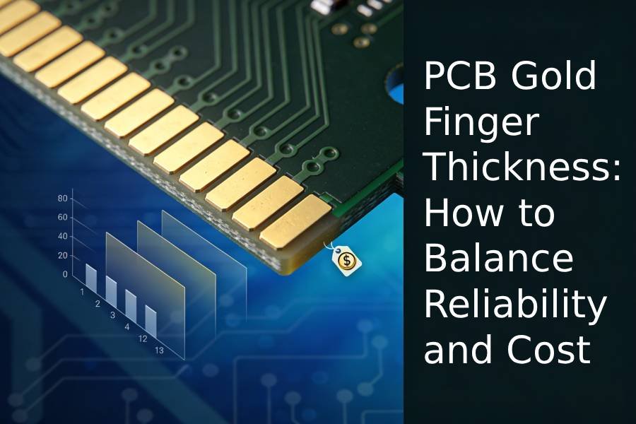
Gold Plating Options & Thickness for Gold Fingers
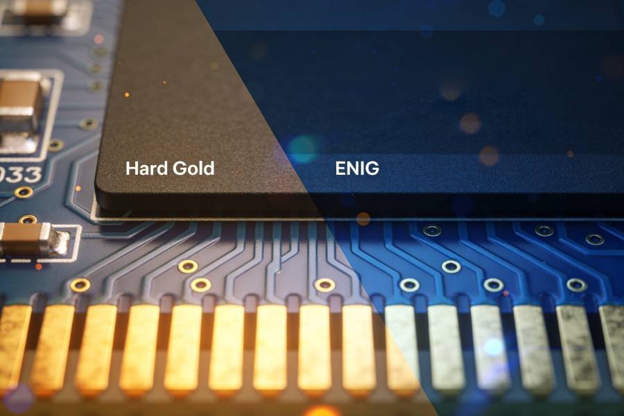
The surface finish on your gold fingers has a direct impact on contact resistance, wear life and overall cost of the PCB. In practice, most edge connectors use either hard electroplated gold or ENIG (electroless nickel immersion gold), and the optimal choice depends on how often the board will be mated, the operating environment and your budget.
For prototypes or low‑cycle applications, ENIG can be a cost‑effective option on the entire board, including the fingers. For production boards that will be plugged in and out many times, hard gold plating on the gold fingers is strongly recommended to ensure long‑term reliability.
Hard Gold vs ENIG
| Item | Hard gold plating on fingers | ENIG on fingers |
|---|---|---|
| Plating method | Electroplated gold over nickel | Electroless nickel, then immersion gold |
| Typical gold thickness | 10–50 µin (up to ~50 µin for high cycles) | 1–3 µin on pads and fingers |
| Wear resistance | Very high, suitable for frequent mating cycles | Moderate, best for low mating cycles and prototypes |
| Contact performance | Very low contact resistance and stable performance over time | Low contact resistance, but thinner gold layer wears faster |
| Typical use on PCB | Local plating only on gold fingers and edge connectors | Whole‑board finish for pads, BGA, fine‑pitch components; sometimes used on fingers for prototypes |
| Reliability in harsh environments | Excellent resistance to oxidation and mechanical wear | Good oxidation resistance, limited mechanical wear life on fingers |
| Relative cost | Higher cost per unit area, but applied only on finger area | Lower cost per unit area, often used on the whole board |
| Recommended applications | Production boards, high mating cycles, industrial and networking equipment | Prototypes, low‑cycle connectors, cost‑sensitive designs where long wear life is not critical |
For most gold finger PCBs, we recommend choosing the gold thickness according to the expected number of mating cycles and the environment. As a general guideline, thinner plating around 3–5 µin is suitable for low‑cycle prototypes, 10–20 µin for medium‑cycle applications, and 30–50 µin for high‑cycle or mission‑critical connectors.
Because we work with multiple manufacturing partners, we can flexibly match the required plating thickness and surface finish for your project instead of forcing you into a single standard. If you share your connector specifications and target lifetime, our engineering team can recommend the most cost‑effective combination of hard gold or ENIG and the appropriate thickness range for your fingers.
Mating cycles vs thickness
| Mating cycles (approx.) | Suggested finish on fingers | Suggested gold thickness |
|---|---|---|
| Prototype / < 50 cycles | ENIG or hard gold | 3–5 µin |
| 50–500 cycles | Hard gold | 10–20 µin |
| 500–1000+ cycles | Hard gold | 30–50 µin |
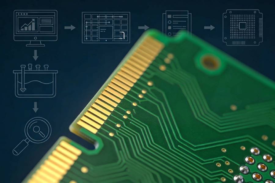
Gold Finger PCB Manufacturing Process
Manufacturing a gold finger PCB follows the standard PCB fabrication flow, with additional steps to build the nickel and gold layers on the edge connector and to bevel the board edge. Below is a typical process used by our manufacturing partners for hard‑gold and ENIG gold fingers.
1. Core PCB fabrication
The PCB stack‑up is produced first, including laminating the cores, etching the copper circuitry, drilling, plating through‑holes and imaging all layers according to your design.
2. Edge connector preparation
Edge Connector Preparation: The board outline is routed and the gold finger edge is defined, leaving clean, exposed copper pads at the connector area.
3. Nickel underlayer plating
A nickel layer is plated onto the copper pads in the gold finger area to act as a barrier and support the final gold layer.
4. Gold plating on fingers
Hard gold or ENIG is applied on top of the nickel to achieve the required thickness, contact performance and wear resistance on the edge connector.
5. Beveling the board edge
The connector edge is beveled, typically at 30°–45°, so the PCB can slide smoothly into the mating slot without damaging the fingers.
6. Solder mask, legend and finishing
Solder mask and silkscreen are applied to the rest of the board while keeping the gold finger area fully exposed and clean.
7. Final inspection and electrical test
The gold finger area is visually inspected for scratches and plating quality, and the finished PCB undergoes electrical testing according to your specifications.
Applications of Gold Finger PCBs
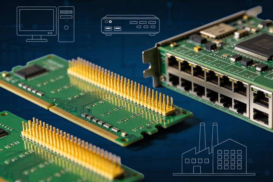
Gold finger PCBs are used wherever you need a compact, reliable and removable electrical connection between two boards or between a board and a slot‑type connector. By routing power, high‑speed signals and control lines through a single edge connector, they make it easy to plug in, upgrade or replace modules without using additional cables.
Technical Applications on the Circuit
- Connecting a daughter board to the main motherboard through an edge connector slot.
- Providing power rails and ground returns to plug‑in modules via the gold fingers.
- Carrying high‑speed data lines between add‑on cards and the baseboard, such as PCIe, memory or I/O interfaces.
- Interconnecting multiple functional blocks on a large system through removable sub‑cards instead of fixed wiring.
- Reserving expansion interfaces so designers can add new features or higher‑performance modules in future product revisions.
Commercial and Industry Use Cases
- Computers & servers – RAM modules, graphics cards, PCI/PCIe expansion cards, storage controllers and other add‑in boards.
- Networking & communications – network interface cards, optical transceiver cards, router and switch line cards, backplane connections.
- Industrial control & automation – PLC I/O cards, motion control cards, fieldbus and communication interface modules.
- Consumer electronics – memory card adapters, docking stations, game console cartridges and accessory boards.
- Measurement, medical and instrumentation – plug‑in data acquisition cards, signal conditioning modules and specialized interface boards.
Because we work with multiple qualified PCB and PCBA factories in China, we can support gold finger PCBs for a wide range of industries, from consumer electronics and computing to industrial, networking and instrumentation projects. Whether you need a single prototype card or a full series of plug‑in modules for mass production, our team can match the right process and surface finish to your application.
Gold Finger PCB Design Checklist (DFM)
Before sending your files for fabrication, it is helpful to run through a short design‑for‑manufacturability (DFM) checklist for the gold finger area. This reduces the risk of production issues, prevents delays and ensures that the edge connector will meet your electrical and mechanical requirements.
- Confirm connector and board thickness
Verify the mating connector type, recommended bevel angle and required board thickness at the gold finger edge so the PCB will fit firmly in the slot. - Define finger count, width and pitch clearly
Make sure the number of fingers, their width and spacing exactly match the connector datasheet and that the pinout is clearly documented. - Choose suitable plating type and thickness
Select hard gold or ENIG for the fingers and specify a gold thickness range that matches the expected mating cycles and environment. - Keep solder mask and silkscreen away from fingers
Ensure the gold finger pads and bevel area are completely free of solder mask and legend so the contact surface is clean and fully exposed. - Avoid vias in or near the gold finger pads
Do not place vias in the pads, and keep any nearby vias at least 0.5–1.0 mm away from the finger area to avoid plating issues and mechanical weakness. - Check copper balance and routing near the edge
Maintain adequate copper clearance from the board edge outside the finger area and avoid sharp right‑angle traces directly at the connector. - Verify layer stack‑up and impedance needs
If high‑speed signals run through the fingers, confirm the stack‑up, reference planes and controlled impedance requirements with the fabricator. - Provide clear fabrication notes
Add notes in the Gerber or fabrication drawing to indicate “gold fingers,” bevel angle, plating requirements and any special inspection needs.
If you are unsure about any of these checklist items, you can simply upload your Gerber files and connector information, and our engineers will perform a free DFM review of the gold finger area before production.
Gold Finger PCB FAQs
For most gold finger PCBs, the typical hard gold thickness ranges from about 3–50 µin on top of a nickel underlayer. Thinner plating around 3–5 µin is often used for prototypes or low mating cycles, while 10–20 µin is common for medium‑duty applications and 30–50 µin is recommended for high‑cycle or mission‑critical connectors.
Hard gold is generally recommended for production boards and any edge connector that will be plugged in and out many times, because it offers excellent wear resistance and very stable contact performance over time. ENIG can be a cost‑effective option for prototypes or low‑cycle connectors, especially when you use it as the main surface finish for the entire board, but its thinner gold layer is not ideal for high mating cycles.
The exact number of mating cycles depends on the gold thickness, the connector design and the operating environment, but properly designed hard‑gold fingers can typically withstand hundreds to around a thousand insertion and removal cycles. If you provide your target lifetime and use conditions, we can recommend a suitable plating thickness and finish to meet those requirements.
Vias should not be placed directly in gold finger pads, because they can cause plating problems, weak mechanical support and unstable contact surfaces. We also recommend keeping any nearby vias at least 0.5–1.0 mm away from the finger area and clearly marking the finger region as a keep‑out zone in your design.
Yes, the gold finger pads and bevel area must be completely free of solder mask and silkscreen so that the connector contacts are clean and fully exposed. Any resist or ink on the fingers can lead to poor contact, higher resistance and premature wear of both the PCB and the mating connector.
For the best results, please include your Gerber or ODB++ files, the desired surface finish on the fingers (hard gold or ENIG), the target gold thickness range, the board thickness at the connector edge and, if possible, the datasheet for the mating connector. Sharing your expected mating cycles and application environment also helps our engineers suggest the most suitable and cost‑effective stack‑up and plating options.
Yes, we offer a free DFM review of the gold finger layout as part of our quoting and engineering support process. Our engineers will check the bevel angle, gold finger length, plating notes, keep‑out areas, via distances and stack‑up information, and then provide feedback or optimization suggestions before the boards are fabricated.
We can support the full range from one‑off prototypes and engineering samples to low‑ and medium‑volume production runs for gold finger PCBs. By working with multiple qualified fabrication and assembly partners in China, we are able to match the right process and capacity to your schedule, budget and technical requirements.
Ready to Start Your Gold Finger PCB Project?
Get DFM‑optimized gold finger PCBs in as fast as 24 hours, from single prototypes to small‑ and medium‑volume production. Our engineering team can review your edge connector design, suggest the right plating and bevel options, and coordinate fabrication and assembly with our qualified partners in China.
Request a Gold Finger PCB Quote
Please fill out the form below and upload your design files. We will review the gold finger area for DFM and send you a detailed quotation, usually within 24 hours.
*Typical response time: within 24 hours on working days.