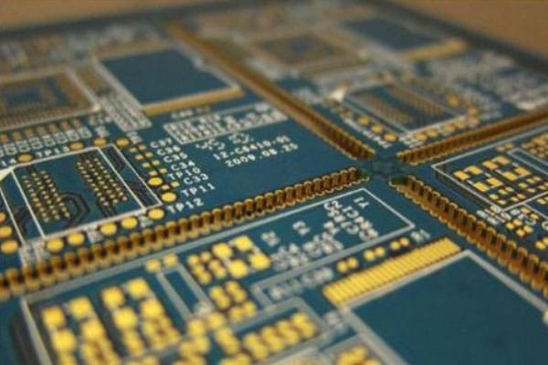
HDI PCB Manufacturing
– Microvia, Blind & Buried Via HDI Boards up to 30 Layers
High-density interconnect (HDI) PCB fabrication with laser-drilled microvias, via-in-pad, and advanced stack-ups for compact, high-performance electronics.
Fast HDI PCB prototyping and production with controlled impedance, strict quality control, and engineering DFM support from China.
- UL, ISO 9001, IATF 16949, RoHS compliant HDI PCB manufacturing.
- Serving automotive, telecom/5G, medical, industrial and consumer electronics brands worldwide.
No minimum order for HDI prototypes, secure file upload, 24‑hour engineering review and quotation.
What is an HDI PCB and Why Choose It for Your Next Design?
High-density interconnect (HDI) PCBs are circuit boards with a much higher wiring density per unit area than conventional PCBs, achieved through microvias, blind and buried vias, fine lines, and thin high-performance materials.
By shortening signal paths, increasing layer usage efficiency, and freeing up routing space under fine-pitch BGAs, HDI PCBs enable more compact, reliable, and higher-speed electronic products.
If your design is pushing limits on size, layer count, or signal integrity, moving to HDI is often the most cost-effective way to keep performance high while keeping the board size and BOM under control.
Why engineers and buyers choose HDI PCBs:
- Pack more functionality into a smaller footprint by using microvias, via-in-pad, and sequential lamination to route high‑pin‑count BGAs and fine‑pitch components efficiently.
- Improve signal integrity and reduce noise by shortening critical high‑speed traces, minimizing stubs, and optimizing return paths through HDI stack-ups.
- Lower overall system cost by reducing the total layer count versus a “standard” multilayer approach or by shrinking board size and enclosure dimensions.
- Enhance reliability with smaller aspect-ratio microvias, better thermal balance, and controlled impedance structures designed for high-speed, high‑frequency operation.
Typical applications where HDI PCBs are the best choice:
- Smartphones, tablets, and wearables that demand ultra‑compact, thin form factors with multiple radios and sensors on one board.
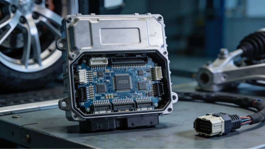
- Automotive electronics including ADAS, infotainment, ECUs, and EV control units that require dense routing and high reliability in harsh environments.
- 5G, networking, and telecom equipment where high‑speed SerDes, RF, and high‑layer‑count backplanes must fit into constrained footprints.
- Medical devices and industrial/IoT systems that combine miniaturization with strict safety, accuracy, and long‑term reliability requirements.
HDI PCB Fabrication Capabilities
Our HDI PCB manufacturing lines are optimized for complex, high‑density designs that need microvias, blind and buried vias, via‑in‑pad, and multiple sequential laminations.
From compact handheld devices to high‑layer‑count telecom and automotive boards, we support advanced HDI stack-ups with fine trace/space, controlled impedance, and reliable microvia structures.
| Capability | Specification (Editable Placeholder) |
|---|---|
| HDI board types | 1+N+1, 2+N+2, 3+N+3, any‑layer / ELIC HDI (rigid and rigid‑flex options) |
| Max HDI layer count | Up to 60‑layer HDI PCBs (evaluation required above 30 layers) |
| Min trace / space | Down to 3/3 mil (0.075 mm) depending on stack-up and material |
| Min mechanical via | e.g. 0.20 mm (7.9 mil) finished hole (adjust to your real spec) |
| Min microvia (laser) | 0.10 mm (4 mil) laser‑drilled microvia, stacked or staggered |
| Via structures | Through, blind, buried, stacked and staggered microvias, via‑in‑pad, copper‑filled vias |
| Sequential lamination | Up to 3+ lamination cycles for complex HDI builds |
| Materials | High‑Tg FR‑4, low‑loss/high‑speed materials, halogen‑free HDI laminates from leading brands |
| Board thickness | Thin HDI cores for handheld devices to thick HDI boards for connectors and backplanes (e.g. 0.4–4.0 mm) |
| Copper thickness | Outer/inner copper options for standard and heavy‑copper HDI designs (e.g. 1/3 oz to 3 oz) |
| Surface finishes | ENIG, ENEPIG, immersion silver, immersion tin, lead‑free HASL, hard gold, gold fingers, OSP etc. |
| Impedance control | Single‑ended and differential impedance with typical ±5–10% tolerance and stack‑up recommendation |
| Solder mask | Multiple colors, fine dam capability for HDI designs with small pads and tight spacing |
To ensure HDI reliability, we combine laser drilling, multiple sequential laminations, resin or copper‑filled microvias, and tight registration control across all layers.
Our CAM and engineering team can review your HDI stack-up, via strategy, and impedance requirements before production, helping you balance manufacturability, cost, and performance for each design.
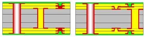
HDI Stackup Options for Different Density and Cost Targets
Choosing the right HDI stackup is critical to balancing density, signal integrity, and cost in your design.
We support mainstream HDI configurations such as 1+N+1, 2+N+2, 3+N+3, and any‑layer (ELIC) HDI so you can match the stackup to your BGA pitch, layer count, and performance requirements.
1+N+1 – Cost‑effective entry HDI
The 1+N+1 HDI stackup adds one build‑up layer with microvias on each side of a conventional multilayer core, giving you a simple and cost‑effective way to escape moderate‑density BGAs.
It is ideal when you need better routing flexibility and size reduction than a standard multilayer PCB, but still want straightforward manufacturing, good yield, and competitive pricing.
- Recommended for BGA pitches around 0.5 mm and designs with medium routing density.
- Great fit for consumer electronics, mid‑range smartphones, IoT controllers, and industrial control boards.
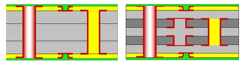
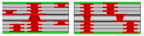
2+N+2 and 3+N+3 HDI – For Fine‑Pitch BGAs and Complex Routing
2+N+2 and 3+N+3 HDI stackups use two or more build‑up layers with microvias on each side of the core, providing much more routing space and flexibility for fine‑pitch, high‑pin‑count components.
These structures help you improve signal integrity, shorten high‑speed paths, and pack significantly more functionality into the same or smaller PCB footprint.
- Recommended for 0.4 mm and below BGA pitch, dense SoC, memory, and high‑speed interface routing.
- Widely used in high‑end smartphones, tablets, 5G modules, networking and data‑center boards, and advanced industrial/automation systems.
Any‑Layer (ELIC) HDI – Maximum Interconnect Density
Any‑layer HDI, also known as ELIC, allows microvias to connect freely between virtually any layers, creating the highest possible interconnect density for extremely complex designs.
This architecture is used when every layer may need to access critical components, and when there is no room for traditional via structures without compromising performance or size.
- Best suited for flagship smartphones, wearables, high‑end computing modules, RF front‑ends, and other space‑constrained, performance‑critical products.
- Often combined with advanced materials and strict process control for premium reliability and signal integrity.
Whether your project needs a cost‑optimized 1+N+1 HDI, a high‑density 2+N+2 or 3+N+3 stackup, or a complex any‑layer HDI architecture, our engineering team can help you select the right build and prepare a production‑ready stackup.
Share your target BGA pitch, layer count, and key interfaces, and we will propose an HDI stackup that balances signal integrity, manufacturability, and total cost of ownership for your design.
Quality, Reliability & DFM Support for HDI PCBs
HDI PCBs push manufacturing limits with ultra‑fine features, stacked microvias, and complex multilayer structures, so process control and testing are critical to long‑term reliability.
We combine strict incoming material control, tightly monitored HDI processes, and multilayer inspection and testing to ensure every HDI board meets your electrical and reliability requirements.
Controlled HDI Processes and Qualified Materials
Our HDI production flow includes controlled laser drilling, precise sequential lamination, advanced desmear and copper plating for microvias, and optimized curing profiles to minimize stress on stacked vias.
We work only with qualified high‑Tg and low‑loss HDI laminate suppliers and maintain detailed process parameters and traceability for each job, so your critical designs are built on a stable and repeatable process window.
Multi‑Stage Inspection and Electrical Testing
To catch defects early and ensure consistent performance, every HDI PCB passes through multiple inspection and test stages.
- Automated optical inspection (AOI) on inner and outer layers to verify fine lines, spacing, pads, and registration before lamination and final finish.
- X‑ray inspection for blind, buried, and stacked microvias to detect voids, misalignment, and plating issues that are invisible on the surface.
- Flying‑probe or fixture‑based electrical testing to check continuity, isolation, and impedance where specified, so every net performs as designed.
- Microsection and cross‑section analysis on representative coupons to confirm via wall thickness, copper fill, layer alignment, and overall HDI structure quality.
HDI‑Focused DFM Review and Engineering Support
Before we start fabrication, our engineering team can run an HDI‑specific DFM review on your Gerber/ODB++/IPC‑2581 data to check trace‑to‑trace spacing, via sizes, annular rings, stackup registration, and other critical constraints.
We provide feedback on microvia aspect ratios, stacked vs staggered via strategies, reference plane placement, and impedance‑controlled layer assignments, helping you improve yield and reliability while avoiding costly redesigns.
If you share your target HDI structure, key interfaces, and reliability requirements, our HDI specialists can recommend a manufacturable stackup, test strategy, and cost‑effective quality level tailored to your project.
HDI PCB Cost & Lead Time
HDI PCB pricing depends on several technical factors including stackup complexity, number of sequential laminations, microvia count and structure, material type, and final yield targets.
By reviewing your design and recommending a cost‑optimized HDI stackup, we help you achieve the right balance between density, performance, and total PCB cost.
Main factors that influence HDI PCB cost:
Typical HDI PCB lead time ranges:
To get an accurate HDI PCB price and delivery estimate, simply upload your Gerber/ODB++/IPC‑2581 files together with your target stackup, materials, and any impedance or reliability requirements.
Our engineers will review your design, suggest cost‑saving options if needed, and send you a detailed HDI PCB quotation and lead time proposal, usually within one business day.
HDI PCB Projects & Industries We Serve
We have manufactured HDI PCBs for a wide range of high‑reliability and space‑constrained products, from handheld devices and medical equipment to automotive and telecom systems.
Our engineering and manufacturing teams work closely with customers to match HDI stackups, materials, and test strategies to the actual end‑use conditions of each project.

Case 1 – Compact medical monitoring device
A customer in the medical sector needed to shrink the size of a portable monitoring device while adding more sensing and wireless functions.
By moving from a conventional multilayer PCB to an HDI stackup with microvias and via‑in‑pad under fine‑pitch BGAs, we helped them reduce board size and improve signal integrity, while meeting their reliability and regulatory requirements.
Case 2 – Automotive / EV control module
An automotive customer required a compact, high‑reliability HDI board for an ECU/ADAS control module operating in a harsh temperature and vibration environment.
We proposed a robust HDI stackup with controlled impedance, optimized microvia structures, and enhanced thermal management, enabling them to integrate more functionality into a smaller module without compromising reliability.
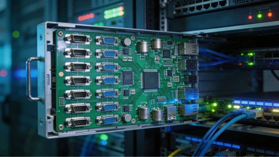
Case 3 – High‑speed networking and 5G board
For a networking/5G application, the design team needed to route multiple high‑speed interfaces and dense BGAs in a limited footprint.
Using a 2+N+2 HDI stackup, low‑loss materials, and carefully planned reference planes, we supported their signal integrity targets while keeping the layer count and PCB size under control.
- Consumer electronics & wearables – HDI PCBs for smartphones, tablets, wearables, cameras, and smart home devices where every millimeter of space matters.
- Automotive & EV – HDI boards for ADAS, infotainment, ECUs, power electronics, and charging systems that must withstand harsh environments and strict safety requirements.
- Medical devices – Compact, high‑reliability HDI PCBs for monitoring devices, diagnostic equipment, and wearable/portable medical electronics.
- Telecom, 5G & networking – High‑layer‑count and high‑speed HDI boards for base stations, small cells, routers, switches, and optical modules.
- Industrial & IoT – HDI PCBs for industrial automation, robotics, sensors, and IoT gateways where density, reliability, and connectivity are critical.
If you share your target industry, application, and basic HDI requirements, we can provide references from similar projects and recommend a proven HDI solution path for your design.
HDI PCB FAQs
HDI PCBs use microvias, blind and buried vias, and finer trace/space to achieve much higher wiring density than standard multilayer PCBs.
This allows you to route more signals in less area, improve signal integrity, and shrink overall board size and weight compared to conventional designs.
You should consider HDI when your design uses fine‑pitch BGAs, needs many high‑speed signals, or must fit more functionality into a smaller footprint than a standard multilayer can handle.
HDI is also recommended when you need better signal integrity, shorter interconnects, or higher reliability in demanding applications such as smartphones, medical, automotive, and 5G/telecom systems.
For a fast and accurate quote, we typically need your Gerber or ODB++/IPC‑2581 data, layer stackup or target layer count, drill/via information, and any special material or impedance requirements.
If you also need assembly, please provide the BOM and pick‑and‑place (XY/centroid) file; if you don’t have complete data yet, you can share a specification, drawing, or sample board so we can discuss options.
Yes, HDI designs require tighter control of trace width/spacing, via sizes and aspect ratios, annular rings, and impedance‑controlled structures than standard boards.
It is strongly recommended to coordinate with our engineering team early in your design to align on manufacturable limits for microvias, stackup, and routing, which helps avoid redesigns and keeps costs under control.
HDI PCBs are generally more expensive per panel than conventional boards because of laser drilling, sequential lamination, microvia filling, and tighter process control.
However, HDI can reduce your total system cost by lowering the layer count, shrinking the board and enclosure size, and enabling higher integration in a single PCB instead of multiple boards and connectors.
Typical lead time for HDI PCB prototypes is around one to two weeks depending on stackup complexity, materials, and our current capacity, with expedited options available after engineering review.
Standard production runs usually take a bit longer than prototypes, especially for very high layer counts or special materials, so we recommend sharing your schedule early so we can plan the best delivery window.
Yes, in addition to HDI bare board fabrication, we can support component sourcing and full PCB assembly when needed, using the same stackup and DFM knowledge gained during fabrication.
Handling both HDI PCB manufacturing and assembly under one roof helps reduce communication gaps, shorten lead times, and improve overall yield and reliability of your project.
Request an HDI PCB Quote
Get a fast, engineering‑driven quotation for your HDI PCB prototype or production build.
Share your design files and basic requirements, and our team will review them and come back with pricing and lead time, usually within one business day.