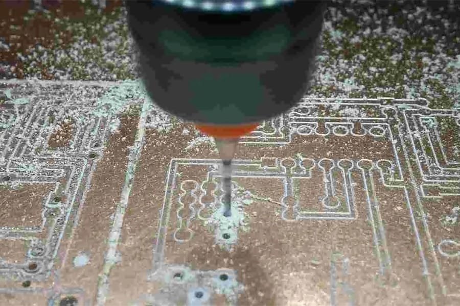
A Complete Guide on PCB Drilling Process
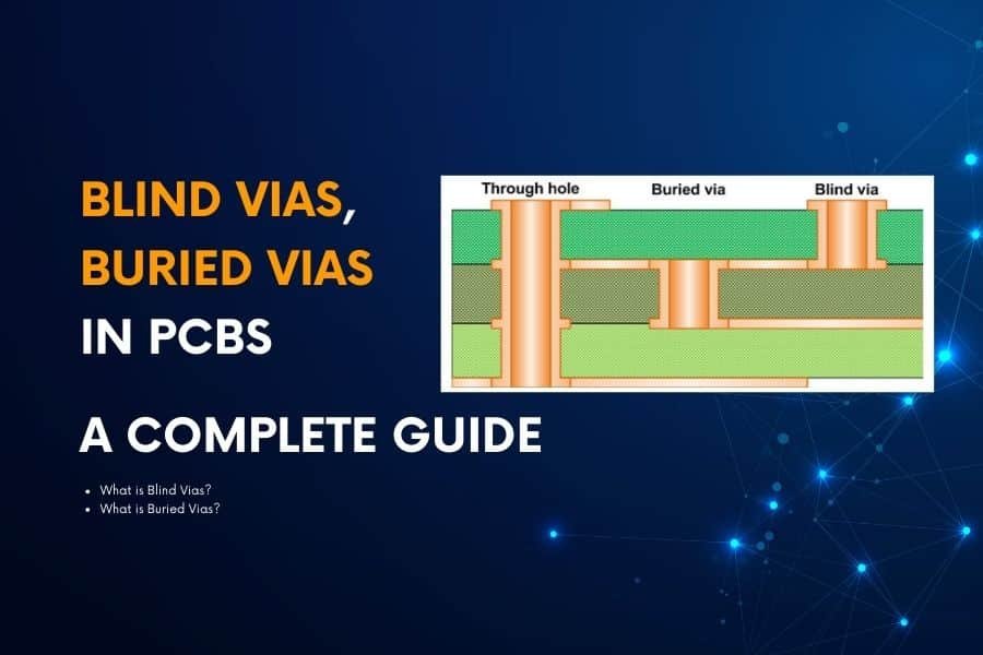
This definitive guide covers all PCB drilling process fundamentals – understanding different hole types like plated through holes (PTHs), preparation steps for quality drilling, mechanical/laser drilling methods, addressing common quality issues, to inspection and improvements. Equip PCB designers, engineers and manufacturers with all the essential knowledge spanning drilling drawings, stack-up, parameters, tool selection to quality control procedures for optimized fabrication.