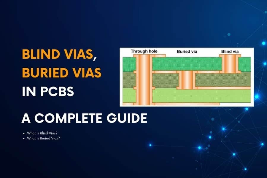
PCB Manufacturing

Plated Through Hole PCB

Understanding Plated Through Holes (PTH) for Printed Circuit Boards

Plated through holes (PTHs) are vital in printed circuit boards for enabling reliable connectivity between layers. This article explores PTHs in depth—from their key benefits like durable interlayer connections and flexible component placement, to critical design considerations around hole size, spacing, depth. We also contrast PTHs to cheaper non-plated holes, and overview popular alternatives like blind and buried vias and their ideal use cases. For PCB designers and manufacturers, our insights help inform effective PTH integration tailored to your product requirements. Reach out to explore our professional PCB fabrication utilizing PTHs.

Understanding Plated Through Holes (PTH) for Printed Circuit Boards Read More »

Solder Mask Line

Navigating The PCB Manufacturing Process Part 4: Solder Mask, Silkscreen, Surface Finish

We have now covered initial PCB production processes – substrate preparation, imaging, plating, etching to form circuitry. The board is now a semi-finished product. This section explains solder mask application to shield copper traces, silkscreen printing for informational markings and labels, and surface metal treatments to protect pads from oxidation while promoting soldering. With these enhancements, boards are fully ready for electronics assembly.

Navigating The PCB Manufacturing Process Part 4: Solder Mask, Silkscreen, Surface Finish Read More »

Pattern Plating Line

Navigating The PCB Manufacturing Process Part 3: Pattern And AOI

We have covered initial PCB production steps – milling, foil lamination, drilling. Now we detail processes to transform base material into functional printed circuit board. First, copper electroplating deposits into drilled holes and grows copper thickness. Photolithography uses UV light to transfer layout pattern onto copper layer. Exposed copper gets etched away, leaving only desired conductive traces. Finally, automated optical inspection compares board to original design to validate quality.

Navigating The PCB Manufacturing Process Part 3: Pattern And AOI Read More »

PCB Fabrication Process

Navigating the PCB Manufacturing Process Part 1: Unveiling MI, Cutting, and Drilling

Dive into the world of PCB manufacturing with our comprehensive guide, focusing on three crucial stages: Manufacturing Instruction (MI), Material Cutting, and Drilling. Join us on a journey through precision and innovation at JHYPCB, where every step in the process plays a vital role in creating high-quality printed circuit boards.

Navigating the PCB Manufacturing Process Part 1: Unveiling MI, Cutting, and Drilling Read More »