Table of Contents
Introduction: The PCB Revolution in the 5G Era
The advent of 5G technology represents one of the most significant technological leaps in telecommunications history, fundamentally reshaping how we connect, communicate, and interact with digital devices. As the fifth generation of wireless technology promises ultra-low latency, massive connectivity, and unprecedented data speeds up to 100 times faster than 4G, it has created a ripple effect across the entire electronics manufacturing ecosystem—with printed circuit boards (PCBs) at the epicenter of this transformation.
The 5G Technology Paradigm Shift
5G technology operates across multiple frequency bands, from sub-6GHz frequencies to millimeter-wave (mmWave) spectrum reaching up to 100GHz. This dramatic expansion in operating frequencies has introduced entirely new challenges and requirements that traditional PCB manufacturing simply cannot address. Unlike previous wireless generations that primarily focused on incremental improvements, 5G demands revolutionary changes in circuit board design, materials, and manufacturing processes.
The technology enables three primary use cases that are driving unprecedented demand for specialized PCBs:
Enhanced Mobile Broadband (eMBB) requires high-frequency PCBs capable of handling massive data throughput while maintaining signal integrity across complex multi-layer structures. Ultra-Reliable Low-Latency Communications (URLLC) demands PCBs with exceptional reliability and minimal signal delay, critical for applications like autonomous vehicles and industrial automation. Massive Machine-Type Communications (mMTC) necessitates cost-effective, power-efficient PCB solutions for billions of IoT devices.
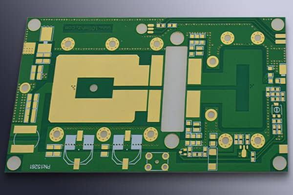
PCBs: The Unsung Heroes of 5G Infrastructure
While much attention focuses on 5G’s visible components—antennas, base stations, and smart devices—PCBs serve as the critical foundation enabling every 5G innovation. These sophisticated circuit boards must simultaneously handle multiple complex functions: managing high-frequency signals without degradation, dissipating increased heat loads, accommodating miniaturized component placement, and maintaining reliability under demanding environmental conditions.
The transition to 5G has created an estimated $15.8 billion global opportunity for PCB manufacturers by 2030, according to industry analysts. This growth stems not just from increased demand, but from the need for entirely new categories of high-performance PCBs that didn’t exist in the 4G era.
What This Comprehensive Analysis Covers
This in-depth exploration examines how 5G technology is fundamentally transforming the PCB industry across multiple dimensions. We’ll investigate the specific technical requirements that 5G imposes on circuit board design and manufacturing, analyze the explosive growth opportunities across different market segments, and explore the innovative solutions that leading PCB manufacturers are developing to meet these challenges.
Our analysis spans from the massive infrastructure buildout of 5G base stations requiring high-power RF PCBs, to the miniaturized antenna modules in smartphones demanding advanced HDI technology, to the emerging applications in autonomous vehicles and Industry 4.0 that are creating entirely new PCB market categories.
For PCB manufacturers, electronics designers, and industry stakeholders, this comprehensive guide provides the strategic insights needed to capitalize on the 5G-driven transformation. We’ll examine not only the opportunities but also the technical challenges, supply chain considerations, and competitive dynamics that will shape the industry’s future.
The 5G revolution is not just changing how we communicate—it’s redefining what’s possible in PCB design and manufacturing. As we stand at the threshold of this technological transformation, understanding these changes is crucial for anyone involved in the electronics manufacturing ecosystem.
Ready to explore how 5G is reshaping the $75 billion global PCB industry? Let’s dive into the technical requirements and market opportunities that are driving this unprecedented growth.

5G's Revolutionary Impact on PCB Technology Requirements
The transition from 4G to 5G represents far more than an incremental upgrade—it demands a complete reimagining of PCB design and manufacturing capabilities. As 5G networks operate across dramatically expanded frequency ranges and support unprecedented data rates, traditional PCB technologies face fundamental limitations that require innovative solutions.
High-Frequency, High-Speed Transmission Demands
1. Understanding 5G Frequency Characteristics
5G technology operates across two primary frequency ranges that present distinct challenges for PCB designers. Sub-6GHz frequencies (typically 3.5-4.9GHz) offer broader coverage and better building penetration, while millimeter-wave frequencies (24-100GHz) provide massive bandwidth but require sophisticated signal management techniques.
At these elevated frequencies, traditional FR4 materials—the workhorse of conventional PCB manufacturing—become inadequate due to excessive signal loss and poor electrical performance. Signal attenuation increases exponentially with frequency, making material selection critical for maintaining signal integrity across complex multi-layer PCB structures.
2. Low-Loss Material Revolution
The shift to 5G has accelerated adoption of advanced low-loss dielectric materials with superior electrical properties:
Rogers Corporation materials such as RO4000 series offer dielectric constants (Dk) as low as 3.38 and dissipation factors (Df) below 0.0027 at 10GHz, representing a 60% improvement in signal loss compared to standard FR4. Taconic’s RF-35 series provides even lower loss characteristics with Df values of 0.0018, crucial for millimeter-wave applications.
Isola’s I-Tera MT40 represents the latest generation of low-loss materials specifically engineered for 5G applications, offering thermal reliability up to 200°C while maintaining consistent electrical properties across the entire 5G frequency spectrum.
However, these advanced materials come with significant cost implications—specialty 5G PCB materials can cost 3-5 times more than traditional FR4, requiring manufacturers to balance performance requirements with economic considerations.
3. Signal Integrity Challenges and Solutions
5G PCBs must address multiple signal integrity issues simultaneously:
Insertion Loss Management: At millimeter-wave frequencies, even minor conductor roughness can cause significant signal attenuation. Advanced reverse-treated copper foils with ultra-smooth surfaces reduce insertion loss by up to 25% compared to standard electrodeposited copper.
Crosstalk Minimization: High-speed 5G signals are particularly susceptible to electromagnetic interference. Optimized layer stackup designs with dedicated ground planes and controlled impedance structures are essential for maintaining signal quality in dense, multi-layer configurations.
Via Design Optimization: Traditional through-hole vias create impedance discontinuities at high frequencies. Microvias and blind/buried via structures in HDI PCBs provide better high-frequency performance while enabling increased routing density.
Miniaturization and Ultra-High-Density Integration
1. HDI Technology Evolution for 5G
The demand for smaller, more capable 5G devices has driven High-Density Interconnect (HDI) technology to new levels of sophistication. Modern 5G smartphones require PCBs with line widths as narrow as 25μm and via diameters under 75μm—pushing the boundaries of conventional manufacturing capabilities.
Any-Layer HDI (ALHDI) technology enables interconnections between any layers in a multilayer PCB stack, providing unprecedented routing flexibility crucial for complex 5G RF circuits. This technology allows designers to create PCBs with 20+ layers while maintaining compact form factors essential for mobile devices.
2. Embedded Component Technology
5G’s miniaturization demands have accelerated adoption of embedded component PCB technology, where passive components are integrated directly into the PCB substrate. This approach offers multiple advantages:
- 50% reduction in PCB footprint compared to surface-mounted equivalents
- Improved high-frequency performance due to shorter interconnection paths
- Enhanced reliability through elimination of solder joints
- Better thermal management through direct substrate contact
Embedded resistor and capacitor technologies using specialty inks and films are becoming standard in 5G antenna matching circuits, where precise component values and minimal parasitic effects are critical.
3. System-in-Package (SiP) Integration
5G applications increasingly rely on System-in-Package (SiP) technology that combines multiple die, passive components, and interconnect structures in a single package. This approach requires PCBs with:
- Ultra-fine pitch ball grid arrays (BGAs) with 0.4mm spacing or smaller
- Advanced via-in-pad technology for maximum connection density
- Precise impedance control across complex 3D interconnect structures
Thermal Management Revolution
1. The 5G Heat Challenge
5G devices generate significantly more heat than their 4G predecessors due to:
- Higher transmission power requirements for millimeter-wave frequencies
- Multiple antenna arrays operating simultaneously in MIMO configurations
- Advanced signal processing requiring high-performance processors
- Increased component density in miniaturized form factors
5G base station power amplifiers can generate heat fluxes exceeding 100W/cm², while smartphone 5G modems produce thermal loads 40% higher than equivalent 4G designs.
2. Thermal Management PCB Solutions
Thermal Interface Materials (TIMs): Advanced PCBs incorporate metal core substrates with aluminum or copper cores providing thermal conductivity up to 200W/mK—nearly 100 times better than standard FR4.
Thermal Vias and Heat Spreaders: Strategic placement of thermal via arrays creates efficient heat conduction paths from high-power components to heat sinks. Copper coin technology embeds thick copper areas directly into PCB layers for localized thermal management.
Advanced Stackup Design: Hybrid metal-core constructions combine the thermal benefits of metal substrates with the electrical properties of low-loss dielectrics, enabling optimal performance for high-power 5G RF circuits.
3. Innovative Cooling Technologies
Cutting-edge 5G PCB designs incorporate liquid cooling channels directly into the PCB substrate, enabling active thermal management for extreme high-power applications. Phase-change material (PCM) integration provides passive thermal buffering for variable load conditions.
The thermal management requirements of 5G have transformed PCB design from a primarily electrical challenge to a complex electro-thermal optimization problem, requiring sophisticated simulation tools and multi-physics design approaches.
These fundamental technological shifts represent just the beginning of 5G’s impact on PCB manufacturing. Next, we’ll explore how these technical requirements translate into explosive growth opportunities across specific market segments.

5G-Driven PCB Market Segments: Unprecedented Growth Opportunities
The technical revolution in 5G PCB requirements has created distinct market segments, each with unique growth trajectories and profit potential. Global 5G PCB market revenue is projected to reach $23.8 billion by 2030, representing a compound annual growth rate (CAGR) of 12.4% from 2024—significantly outpacing the broader PCB industry’s 5.2% CAGR.
Communication Infrastructure: The Foundation of 5G Growth Base Station PCB Market Explosion
The 5G base station PCB market represents the largest and fastest-growing segment within communication infrastructure, driven by massive global network deployments. Industry analysts project this segment will reach $8.2 billion by 2028, with China, the United States, and Europe leading infrastructure investments.
Macro Base Station Requirements: 5G macro base stations demand high-power RF PCBs capable of handling transmission powers up to 200W per channel. These applications require:
- Multi-layer PCBs (12-20 layers) with specialized high-frequency stackups
- Thick copper constructions (3-6oz) for power distribution and thermal management
- Advanced materials such as Rogers RO4350B or Isola I-Speed for low-loss performance
- Specialized surface finishes like ENIG (Electroless Nickel Immersion Gold) for reliable RF connections
The average selling price (ASP) for macro base station PCBs ranges from $150-400 per board, significantly higher than consumer electronics PCBs due to material costs and manufacturing complexity.
Small Cell and Distributed Antenna Systems: The shift toward small cell networks for urban 5G coverage creates a different PCB opportunity. Small cell base stations require:
- Compact, cost-optimized designs with 6-10 layer constructions
- Integrated antenna PCBs combining RF circuitry with radiating elements
- Weather-resistant materials for outdoor deployment
- Volume production capabilities as operators deploy thousands of units per city
Market research indicates small cell PCB demand will grow 18% annually through 2028, driven by urban densification requirements and indoor coverage solutions.
5G Core Network Infrastructure
The evolution to 5G Standalone (SA) architecture requires completely new core network infrastructure, creating substantial PCB opportunities in:
Edge Computing Servers: 5G’s ultra-low latency promises require processing power at network edges, driving demand for high-speed digital PCBs with:
- Controlled impedance designs for 56Gbps+ data rates
- Advanced via structures to minimize signal degradation
- Thermal management solutions for high-density processor configurations
Network Function Virtualization (NFV) Hardware: Virtualized 5G networks require specialized server PCBs optimized for telecommunications workloads, representing a $2.1 billion market opportunity by 2027.
Terminal Equipment: Consumer and Enterprise Device Revolution Smartphone 5G PCB Innovation
1. Smartphone 5G PCB Innovation
The smartphone 5G PCB market faces unique challenges combining advanced RF performance with extreme miniaturization. Premium 5G smartphone PCBs can cost 2-3 times more than equivalent 4G designs due to:
Advanced Antenna Integration: 5G smartphones incorporate 4-8 antenna modules for different frequency bands and MIMO configurations. Each antenna module requires:
- Ultra-thin flexible PCBs (as thin as 0.06mm) for space-constrained designs
- Liquid Crystal Polymer (LCP) substrates for millimeter-wave applications
- Precision impedance matching circuits using embedded components
- Multi-band functionality covering sub-6GHz and mmWave frequencies simultaneously
RF Front-End Complexity: 5G smartphones require sophisticated RF front-end modules with PCB demands including:
- HDI technology with 75μm microvias and 25μm line widths
- Advanced shielding solutions to prevent interference between multiple radios
- Thermal management for power amplifiers generating increased heat
The 5G smartphone PCB market is projected to reach $4.7 billion by 2026, with flagship devices driving adoption of premium PCB technologies.
2. IoT and Connected Device Proliferation
5G-enabled IoT devices represent a massive volume opportunity with different PCB requirements:
Industrial IoT Applications: Require ruggedized PCBs with:
- Extended temperature ratings (-40°C to +125°C)
- High reliability standards (automotive-grade or better)
- Cost optimization for large-scale deployments
- Power efficiency for battery-operated sensors
Smart City Infrastructure: Including traffic management, environmental monitoring, and security systems, requires specialized outdoor PCBs with:
- Conformal coating compatibility for weather protection
- Long-term reliability (10+ year operating life)
- Standardized form factors for interoperability
Market projections indicate 5G IoT PCB demand will grow 22% annually, making it one of the fastest-expanding segments.
Emerging High-Growth Applications
1. Autonomous Vehicle Communication Systems
The convergence of 5G and autonomous driving creates entirely new PCB market categories:
Vehicle-to-Everything (V2X) Communication: Automotive 5G PCBs must meet stringent AEC-Q100 qualification standards while providing:
- Ultra-reliable connectivity for safety-critical applications
- Low-latency performance for real-time decision making
- Multi-standard support (5G NR, C-V2X, Wi-Fi 6E)
- Automotive temperature cycling (-40°C to +150°C)
In-Vehicle Networks: 5G-enabled vehicles require high-speed backbone PCBs for:
- Ethernet switching at 10Gbps+ speeds for sensor data
- Gateway functions connecting multiple vehicle networks
- Over-the-air update capabilities requiring secure boot implementations
The automotive 5G PCB market is projected to reach $1.8 billion by 2030, with luxury and premium vehicles leading adoption.
2. Industry 4.0 and Smart Manufacturing
5G-enabled manufacturing requires specialized PCB solutions for:
Edge Computing Platforms:
- Ruggedized designs for factory environments
- Real-time processing capabilities for machine control
- Modular architectures for flexible deployment
Wireless Sensor Networks:
- Ultra-low power designs for battery operation
- Mesh networking capabilities for factory-wide coverage
- Predictive maintenance functionality requiring sensor fusion
Collaborative Robotics:
- High-reliability PCBs for safety-critical applications
- Real-time communication for coordinated robot operations
- Advanced sensor integration for environment awareness
3. Private 5G Network Equipment
Enterprise private 5G networks represent a rapidly emerging market segment requiring:
- Campus-scale base stations with moderate power requirements
- Enterprise gateway equipment for network management
- Specialized CPE devices for industrial applications
Market analysts project private 5G PCB demand will grow 35% annually through 2028, driven by manufacturing, logistics, and healthcare sector adoption.
4. Market Segment Summary and Growth Projections
| Market Segment | 2024 Market Size | 2030 Projection | CAGR | Key Drivers |
|---|---|---|---|---|
| Base Station PCBs | $3.2B | $8.2B | 17.2% | Infrastructure buildout |
| Smartphone PCBs | $2.8B | $4.7B | 9.1% | 5G device upgrades |
| IoT Device PCBs | $0.8B | $2.4B | 22.1% | Massive IoT deployment |
| Automotive PCBs | $0.4B | $1.8B | 28.3% | Autonomous vehicle adoption |
| Industrial PCBs | $0.6B | $1.9B | 21.2% | Industry 4.0 transformation |
These diverse market opportunities require different PCB manufacturing capabilities and business strategies. Understanding the specific requirements of each segment is crucial for manufacturers looking to capitalize on 5G growth.
5G PCB Manufacturing: Technical Challenges and Innovative Solutions
The transition to 5G PCB manufacturing presents unprecedented technical challenges that demand revolutionary approaches to materials, processes, and quality control. Successful 5G PCB manufacturers must master complex technologies that were previously confined to specialized aerospace and military applications, while achieving the cost efficiency required for commercial markets.
Advanced Material Technologies and Selection Strategies
1. Breaking Through Traditional Material Limitations
The inadequacy of conventional FR4 materials at 5G frequencies has forced the industry to adopt next-generation dielectric materials with superior electrical and thermal properties. However, this transition brings significant challenges in material handling, processing, and cost management.
Low-Loss Dielectric Material Evolution:
Rogers Corporation’s Advanced Solutions:
- RO4350B: Offers exceptional thermal stability with a Tg of 280°C and maintains consistent electrical properties across the 5G spectrum (Dk=3.48±0.05, Df=0.0031 at 10GHz)
- RO4835T: Provides lower loss characteristics (Df=0.0022) specifically engineered for millimeter-wave applications
- RT/duroid 5880: Delivers industry-leading low loss (Df=0.0009) for the most demanding 5G base station applications
Taconic’s Specialized RF Materials:
- TLY-5A: Combines low loss (Df=0.0018) with excellent thermal conductivity (0.69 W/mK) for high-power applications
- CER-10: Offers ultra-low loss (Df=0.0035) with ceramic-filled construction for enhanced dimensional stability
Isola’s Next-Generation Portfolio:
- I-Tera MT40: Features breakthrough low loss (Df=0.0031) with traditional FR4 processing compatibility
- Astra MT77: Provides excellent high-frequency performance with reduced material costs compared to PTFE-based alternatives
2. Material Cost Management Strategies
The 3-5x cost premium of 5G materials compared to FR4 requires innovative approaches:
Hybrid Stackup Design: Combining high-performance materials only in critical RF layers with cost-effective materials in digital sections can reduce overall material costs by 40-60% while maintaining performance.
Volume Procurement Strategies: Leading manufacturers establish strategic partnerships with material suppliers to secure consistent supply and preferential pricing for high-volume 5G programs.
Design Optimization: Advanced electromagnetic simulation tools enable material usage optimization, using premium materials only where essential for electrical performance.
3. Material Processing Challenges
5G materials require specialized handling and processing techniques:
Dimensional Stability: Many low-loss materials exhibit different thermal expansion characteristics than FR4, requiring precise compensation in artwork scaling and specialized lamination profiles.
Adhesion and Reliability: PTFE-based materials require surface treatment for reliable copper adhesion, while maintaining low-loss characteristics essential for 5G performance.
Environmental Considerations: Next-generation halogen-free, low-loss materials address environmental regulations while maintaining 5G performance requirements, though often at premium costs.
Revolutionary Manufacturing Process Innovations
1. Precision Fabrication for Ultra-Fine Features
5G PCB manufacturing demands precision levels previously reserved for semiconductor fabrication:
Advanced Lithography Systems:
- Laser Direct Imaging (LDI) systems with 1μm resolution capability for ultra-fine line formation
- Advanced photoresist systems optimized for high-aspect-ratio features required in HDI constructions
- Automated optical inspection (AOI) with sub-micron accuracy for quality verification
Ultra-Fine Line/Space Capabilities: Modern 5G PCB facilities achieve 15μm line/space geometries using:
- Pulse-reverse copper plating for uniform conductor formation
- Advanced etching chemistries providing precise conductor profile control
- Substrate pre-treatment processes ensuring optimal adhesion at fine geometries
2. Advanced Via Technology Implementation
Laser Drilling Precision: 5G HDI PCBs require microvias as small as 50μm diameter with aspect ratios up to 1:1. Achieving these specifications demands:
- UV laser drilling systems with 355nm wavelength for clean via formation in organic materials
- CO2 laser processing for selective material removal in complex stackups
- Sequential build-up processes enabling any-layer interconnect capabilities
Via Filling and Planarization:
- Conductive paste filling for reliable electrical connections in high-aspect-ratio vias
- Copper plating optimization preventing void formation in small-diameter vias
- Surface planarization techniques ensuring flat surfaces for subsequent layer lamination
3. Multilayer Construction Mastery
5G applications frequently require 20+ layer PCBs with complex mixed-material stackups:
Advanced Lamination Technology:
- Vacuum lamination systems preventing air entrapment in complex stackups
- Precise temperature profiling accommodating different material thermal requirements
- Pressure distribution optimization ensuring uniform layer adhesion across large panels
Layer Registration Accuracy:
- Advanced optical alignment systems achieving ±25μm layer-to-layer registration
- Thermal compensation algorithms accounting for material movement during processing
- Real-time monitoring systems detecting and correcting registration drift
4. Surface Finish Optimization for High-Frequency Performance
5G PCBs require specialized surface finishes that maintain electrical performance while providing reliable component attachment:
ENIG (Electroless Nickel Immersion Gold) Optimization:
- Controlled nickel thickness (3-6μm) minimizing skin effect losses at high frequencies
- Ultra-thin gold deposits (0.05-0.1μm) reducing cost while maintaining solderability
- Process control systems ensuring uniform deposit thickness across large panels
Alternative Advanced Finishes:
- Immersion Silver (IAg): Provides excellent high-frequency performance at lower cost than ENIG
- Organic Solderability Preservative (OSP): Optimized formulations for high-frequency applications
- Direct Immersion Gold (DIG): Eliminates nickel layer for ultimate high-frequency performance
Quality Control and Testing Revolution
1. High-Frequency Testing Methodologies
Traditional PCB testing methods prove inadequate for 5G applications, requiring sophisticated RF characterization techniques:
Vector Network Analyzer (VNA) Testing:
- Broadband characterization from DC to 110GHz for complete 5G spectrum coverage
- S-parameter measurements providing comprehensive transmission line characterization
- Time-domain analysis identifying specific impedance discontinuities and reflections
Advanced Test Structures:
- Coupon-based test vehicles incorporating representative 5G circuit geometries
- Embedded test structures enabling in-situ performance verification
- Statistical process control using high-frequency measurements for process optimization
2. Signal Integrity Verification
Eye Diagram Analysis: High-speed digital portions of 5G PCBs require comprehensive signal integrity verification:
- Bit error rate testing (BERT) at data rates up to 112Gbps
- Jitter analysis identifying sources of signal degradation
- Channel compliance testing verifying adherence to 5G interface standards
Electromagnetic Compatibility (EMC) Testing:
- Near-field scanning identifying potential interference sources
- Radiated emissions testing ensuring regulatory compliance
- Immunity testing verifying robust operation in electromagnetic environments
3. Reliability and Environmental Testing
5G PCBs must demonstrate exceptional reliability across diverse operating conditions:
Accelerated Life Testing:
- Thermal cycling from -55°C to +150°C for automotive applications
- Humidity resistance testing simulating tropical deployment conditions
- Vibration and shock testing for mobile and transportation applications
Long-Term Reliability Assessment:
- Highly Accelerated Life Testing (HALT) identifying potential failure mechanisms
- Step-stress testing determining operational limits and design margins
- Failure analysis capabilities using advanced analytical techniques (SEM, X-ray, cross-sectioning)
4. Process Control and Automation
Real-Time Monitoring Systems:
- In-line measurement systems tracking critical parameters throughout manufacturing
- Statistical process control (SPC) identifying process variations before they impact quality
- Automated feedback systems providing real-time process adjustments
Traceability and Documentation:
- Complete genealogy tracking from raw materials through final test
- Automated data collection reducing human error and improving consistency
- Customer-specific reporting providing detailed quality documentation for critical applications
5. Manufacturing Excellence in the 5G Era
The complexity of 5G PCB manufacturing requires integrated approaches combining advanced materials, precision processes, and sophisticated quality control. Successful manufacturers invest in:
- Continuous technology upgrades staying ahead of evolving 5G requirements
- Skilled workforce development training technicians in advanced manufacturing techniques
- Strategic supplier partnerships ensuring access to cutting-edge materials and equipment
- Customer collaboration developing optimized solutions for specific 5G applications
These manufacturing innovations represent the foundation for capturing 5G PCB market opportunities. Next, we’ll examine the competitive landscape and strategic positioning required for success in this rapidly evolving market.

Market Opportunities and Competitive Landscape in the 5G PCB Era
The 5G PCB market presents a complex competitive landscape where traditional market leaders face challenges from specialized manufacturers, while new opportunities emerge for companies that can master advanced technologies and strategic positioning. Understanding this evolving ecosystem is crucial for manufacturers seeking to capitalize on 5G’s $23.8 billion PCB market opportunity.
Global Market Analysis and Regional Dynamics
1. Comprehensive Market Size and Growth Projections
Global 5G PCB Market Overview (2024-2030): The worldwide 5G PCB market demonstrates exceptional growth momentum across all major segments:
| Year | Market Size (USD Billion) | YoY Growth | Key Growth Driver |
|---|---|---|---|
| 2024 | $8.4B | 15.2% | Infrastructure rollout |
| 2025 | $10.1B | 20.1% | Consumer device adoption |
| 2026 | $12.5B | 23.8% | Enterprise deployment |
| 2027 | $15.9B | 27.2% | Automotive integration |
| 2028 | $19.2B | 20.8% | IoT mass deployment |
| 2029 | $21.8B | 13.5% | Market maturation |
| 2030 | $23.8B | 9.2% | Technology evolution |
Regional Market Distribution and Opportunities:
Asia-Pacific (55% Market Share – $13.1B by 2030): The APAC region dominates global 5G PCB manufacturing due to:
- China’s massive 5G infrastructure investment ($180B committed through 2025)
- Advanced manufacturing capabilities in Taiwan, South Korea, and Japan
- Cost-competitive production for volume consumer electronics
- Integrated supply chain ecosystems supporting rapid innovation cycles
Key Growth Markets:
- China: Leading in base station PCB demand ($4.2B by 2030)
- South Korea: Premium smartphone PCB innovation hub
- Taiwan: Advanced HDI and IC substrate manufacturing
- Japan: High-reliability automotive and industrial PCBs
North America (25% Market Share – $5.9B by 2030): North American opportunities focus on:
- High-value, low-volume applications (defense, aerospace, medical)
- Private 5G network infrastructure for enterprise customers
- Automotive 5G integration led by Detroit’s automotive industry
- Advanced R&D and prototyping services for leading technology companies
Europe (15% Market Share – $3.6B by 2030): European market characteristics include:
- Automotive 5G PCBs driven by German premium manufacturers
- Industrial IoT applications supporting Industry 4.0 initiatives
- Regulatory-compliant designs meeting strict environmental standards
- High-reliability applications for critical infrastructure
Rest of World (5% Market Share – $1.2B by 2030): Emerging opportunities in:
- India: Rapidly expanding 5G infrastructure deployment
- Brazil: Smart city and telecommunications infrastructure
- Middle East: Oil & gas industry digital transformation
2. Market Penetration by Application Segment
Infrastructure Equipment (40% of market):
- Macro base stations: $3.8B opportunity (premium pricing, moderate volume)
- Small cell equipment: $2.1B opportunity (cost-sensitive, high volume)
- Core network equipment: $1.9B opportunity (high-performance, specialized)
Consumer Electronics (35% of market):
- Premium smartphones: $4.2B opportunity (technology leadership, margins)
- Tablets and laptops: $1.8B opportunity (performance differentiation)
- Wearable devices: $1.3B opportunity (miniaturization premium)
Automotive and Transportation (15% of market):
- Connected vehicles: $2.4B opportunity (highest growth rate, +28% CAGR)
- Fleet management: $0.8B opportunity (B2B focus, recurring revenue)
Industrial and Enterprise (10% of market):
- Private 5G networks: $1.6B opportunity (customization premium)
- Industrial automation: $0.9B opportunity (reliability requirements)
Supply Chain Analysis and Strategic Partnerships
1. Critical Supply Chain Dependencies
Raw Material Supply Chain Challenges: The 5G PCB industry faces unprecedented supply chain complexity due to specialized material requirements:
High-Frequency Substrate Materials:
- Limited supplier base: Rogers, Taconic, and Isola control 75% of advanced materials
- Long lead times: 12-16 weeks for specialty materials vs. 4-6 weeks for FR4
- Price volatility: Material costs fluctuate 15-25% based on supply/demand dynamics
- Qualification requirements: New materials require 6-12 months customer qualification
Strategic Implications: Leading manufacturers implement dual-sourcing strategies and maintain strategic inventory buffers of critical materials, despite carrying costs of 8-12% annually.
Copper Foil and Specialty Components:
- Ultra-smooth copper foils for high-frequency applications face supply constraints
- Specialty connectors and components require long-term supplier relationships
- Quality certifications for automotive and aerospace applications add complexity
2. Equipment and Technology Partnerships
Manufacturing Equipment Dependencies: 5G PCB production requires substantial capital investments in specialized equipment:
Critical Manufacturing Systems:
- Advanced drilling systems: $2-4M investment per line for laser drilling capabilities
- High-speed plating lines: $5-8M for precision copper deposition systems
- Advanced testing equipment: $1-3M for high-frequency characterization capabilities
Technology Partnership Strategies: Successful manufacturers develop strategic alliances with:
- Equipment suppliers: Joint development programs for next-generation capabilities
- Material suppliers: Early access to advanced materials and technical support
- Test equipment vendors: Customized solutions for 5G-specific applications
- Software providers: Advanced simulation and design optimization tools
3. Customer Relationship Management
Key Customer Segments and Requirements:
Tier-1 Telecommunications Equipment Manufacturers: Companies like Ericsson, Nokia, and Huawei demand:
- Global manufacturing footprint for supply chain security
- Advanced quality systems (ISO 9001, TL 9000, AS9100)
- Technology roadmap alignment for future 5G evolution
- Cost reduction partnerships achieving 3-5% annual productivity improvements
Leading Smartphone OEMs: Apple, Samsung, and other premium brands require:
- Cutting-edge technology access to maintain competitive advantage
- Volume scalability supporting millions of units annually
- Supply chain transparency for corporate responsibility reporting
- Innovation partnerships for next-generation product development
Competitive Strategy Framework for 5G Success
1. Technology Differentiation Strategies
Advanced Capability Development: Companies achieving 5G market leadership focus on distinctive technical capabilities:
Ultra-High-Frequency Expertise:
- Millimeter-wave PCB mastery (24-100GHz applications)
- Advanced simulation capabilities using 3D electromagnetic modeling
- Proprietary design techniques for signal integrity optimization
- Specialized test methodologies for comprehensive characterization
Manufacturing Excellence:
- Industry 4.0 integration using IoT sensors and AI-driven process control
- Zero-defect quality systems achieving <10 PPM defect rates
- Rapid prototyping capabilities with 5-7 day turnaround times
- Flexible manufacturing systems supporting both prototype and volume production
2. Cost Leadership Through Innovation
Operational Excellence Initiatives: Leading manufacturers achieve sustainable cost advantages through:
Process Optimization:
- Lean manufacturing implementation reducing waste and cycle times
- Automation integration minimizing labor content and improving consistency
- Yield improvement programs targeting >95% first-pass yields
- Energy efficiency initiatives reducing manufacturing costs and environmental impact
Scale Economics:
- Capacity utilization optimization maintaining >85% equipment utilization
- Supplier consolidation leveraging volume for preferential pricing
- Standardization programs reducing complexity and setup times
- Shared services implementation for support functions across facilities
3. Customer Intimacy and Solution Development
Value-Added Service Portfolio: Successful 5G PCB manufacturers differentiate through comprehensive solution offerings:
Design and Engineering Services:
- Co-development partnerships with leading technology companies
- Design for manufacturability (DFM) optimization reducing costs and improving yields
- Simulation and modeling services predicting performance before fabrication
- Technology consulting helping customers navigate 5G design challenges
Supply Chain Integration:
- Component sourcing and procurement leveraging manufacturer relationships
- Inventory management services reducing customer working capital requirements
- Logistics optimization providing just-in-time delivery capabilities
- Quality assurance programs ensuring consistent performance across suppliers
4. Market Entry and Expansion Strategies
Geographic Expansion Approaches: Companies entering new 5G PCB markets should consider:
Organic Growth Strategies:
- Greenfield facility development in high-growth regions
- Technology transfer programs replicating proven capabilities
- Local talent acquisition building regional expertise and customer relationships
- Regulatory compliance programs meeting local standards and certifications
Inorganic Growth Options:
- Strategic acquisitions of specialized technology companies
- Joint venture formations with regional partners
- Technology licensing agreements accessing patented innovations
- Distribution partnerships leveraging established customer relationships
5. Competitive Success Factors Summary
The 5G PCB market rewards companies that successfully combine:
- Advanced technical capabilities in high-frequency design and manufacturing
- Operational excellence achieving cost leadership and quality superiority
- Strategic partnerships across the supply chain and customer base
- Innovation culture driving continuous technology advancement
- Global presence supporting multinational customer requirements
- Financial strength funding required technology investments and market expansion
Companies mastering these success factors position themselves to capture disproportionate value from the 5G transformation. Our final sections will explore future trends and provide strategic recommendations for navigating this dynamic market landscape.
Industry Development Trends and Future Outlook
The 5G PCB industry stands at a pivotal moment where emerging technologies, evolving market dynamics, and sustainability imperatives are reshaping the landscape. As we look toward the next decade, several transformative trends will define the trajectory of PCB manufacturing and applications in the 5G ecosystem.
Technology Development Trends
1. 6G Technology Preview: The Next Frontier
While 5G deployment continues globally, forward-thinking PCB manufacturers are already preparing for 6G technology, expected to emerge commercially by 2030. Early 6G research indicates revolutionary requirements that will push PCB technology to new limits.
Terahertz Frequency Challenges
6G networks will likely operate in the terahertz frequency range (0.1-10 THz), presenting unprecedented material science challenges. At these frequencies, current low-loss materials like Rogers RO4000 series may prove insufficient, necessitating entirely new substrate materials with:
- Ultra-low dielectric loss (Df < 0.001)
- Exceptional dimensional stability at molecular levels
- Novel polymer compositions incorporating graphene or carbon nanotube reinforcements
- Manufacturing processes capable of maintaining tolerances within nanometer precision
Space-Air-Ground Integrated Communications
6G’s vision of ubiquitous connectivity will integrate terrestrial, aerial, and satellite networks, creating unique PCB requirements:
- Satellite Communication PCBs: Designed for extreme temperature variations (-150°C to +150°C) and radiation resistance
- High-Altitude Platform Station (HAPS) PCBs: Lightweight designs for stratospheric communications platforms
- Underwater Communications: Specialized substrates for maritime and underwater IoT applications
The PCB industry must begin investing in research and development now to meet these future demands, with early adopters likely to capture significant market share.
2. AI-Driven PCB Design Revolution
Artificial intelligence is transforming PCB design from a largely manual process to an intelligent, automated workflow that promises to reduce development cycles by 60-70% while improving performance and reliability.
Automated Design Optimization
Machine learning algorithms are revolutionizing circuit layout optimization:
- Placement Algorithms: AI systems can analyze millions of component placement combinations to minimize signal path lengths and electromagnetic interference
- Routing Optimization: Neural networks trained on high-frequency design principles automatically generate optimal trace routing with minimal human intervention
- Thermal Management: AI-powered thermal simulation predicts hot spots and automatically adjusts copper fill patterns and via placement for optimal heat dissipation
Leading EDA software providers like Cadence, Synopsys, and Altium are integrating AI capabilities, with some reporting 40% faster design completion times and 25% improvement in first-pass success rates.
Predictive Manufacturing and Quality Control
AI applications extend beyond design into manufacturing:
- Defect Prediction: Machine learning models analyze historical production data to predict potential defect locations before manufacturing begins
- Process Optimization: Real-time AI monitoring adjusts etching parameters, drilling speeds, and lamination pressures to maintain optimal quality
- Yield Enhancement: Predictive analytics identify process variations that impact yield, enabling proactive adjustments
Companies implementing AI-driven manufacturing report 15-30% improvements in yield rates and 50% reduction in quality-related rework.
3. Sustainable Manufacturing and Green Technology
Environmental sustainability has evolved from a regulatory requirement to a competitive advantage, driving innovation in materials, processes, and product lifecycle management.
Revolutionary Green Materials
The PCB industry is pioneering eco-friendly alternatives to traditional materials:
- Bio-based Substrates: Plant-derived polymers and natural fiber reinforcements are replacing petroleum-based materials, with some bio-substrates achieving comparable electrical performance to conventional FR-4
- Recyclable Thermoset Materials: Development of chemically recyclable thermoset resins enables true circular economy principles in PCB manufacturing
- Halogen-Free Solutions: Complete elimination of halogenated flame retardants without compromising fire safety, driven by European RoHS regulations and corporate sustainability goals
Carbon Footprint Reduction Strategies
Manufacturing process innovations focus on energy efficiency and emission reduction:
- Low-Temperature Processing: New cure chemistries enable lamination at temperatures 50°C lower than traditional processes, reducing energy consumption by 20-25%
- Solvent-Free Processes: Dry film resist technologies and solvent-free cleaning processes eliminate volatile organic compound emissions
- Renewable Energy Integration: Leading manufacturers are transitioning to 100% renewable energy, with some achieving carbon-neutral production
Circular Economy Implementation
Progressive PCB manufacturers are implementing comprehensive circular economy models:
- Design for Disassembly: PCB architectures that facilitate component recovery and material separation at end-of-life
- Material Recovery Programs: Closed-loop systems that recover copper, gold, and rare earth elements from production waste and end-of-life products
- Remanufacturing Initiatives: Refurbishment programs that extend PCB lifecycle in less demanding applications
Market Development Predictions
1. Five-Year Growth Trajectory (2025-2030)
The 5G PCB market is entering a mature growth phase characterized by application diversification and geographical expansion.
Market Size Evolution
Based on current deployment rates and emerging applications, the global 5G PCB market is projected to experience robust growth:
- 2025: $420 billion (base case scenario)
- 2027: $580 billion (driven by automotive and industrial IoT adoption)
- 2030: $850 billion (including early 6G infrastructure investment)
This represents a compound annual growth rate (CAGR) of 22-28%, significantly outpacing the broader PCB market growth of 4-6%.
Regional Market Dynamics
Asia-Pacific Dominance Continues The Asia-Pacific region will maintain its leadership position, accounting for approximately 68% of global 5G PCB production by 2030:
- China: Transition from manufacturing hub to innovation center, with domestic companies capturing 45% of high-end 5G PCB market
- South Korea: Technology leadership in advanced packaging and semiconductor integration
- Japan: Premium materials and precision manufacturing equipment supply
- Southeast Asia: Emerging as cost-effective manufacturing base for standard 5G PCBs
North American Market Transformation The North American market will focus on high-value applications and technology development:
- Defense and aerospace applications driving demand for ultra-reliable 5G PCBs
- Reshoring initiatives creating domestic manufacturing capacity for critical applications
- Investment in advanced manufacturing technologies and automation
European Market Specialization Europe will leverage its automotive industry strength and environmental leadership:
- Automotive 5G applications representing 35% of European 5G PCB demand by 2030
- Leadership in sustainable manufacturing practices and green PCB technologies
- Strong regulatory framework driving innovation in eco-friendly materials
2. Emerging Application Scenarios
Several breakthrough applications will drive 5G PCB demand beyond traditional telecommunications infrastructure.
Extended Reality (XR) Ecosystems
The convergence of virtual reality (VR), augmented reality (AR), and mixed reality (MR) will create substantial PCB opportunities:
- Ultra-Low Latency Requirements: XR applications demand sub-5ms latency, requiring specialized PCB designs optimized for high-speed signal processing
- Miniaturization Challenges: Wearable XR devices necessitate flexible-rigid PCB combinations and advanced HDI technologies
- Market Potential: The XR PCB market is projected to reach $12 billion by 2030, growing at 45% CAGR
Digital Twin Infrastructure
Industrial digital twin implementations will drive demand for edge computing PCBs:
- Real-time Data Processing: PCBs designed for AI inference chips and high-speed data acquisition
- Environmental Resilience: Industrial-grade PCBs capable of operating in harsh manufacturing environments
- Scalability Requirements: Modular PCB architectures that support system expansion and upgrade
Autonomous Systems Integration
Beyond automotive applications, autonomous systems will expand into multiple sectors:
- Delivery Drones: Lightweight, power-efficient PCBs for commercial delivery systems
- Agricultural Robots: Ruggedized PCBs for precision farming applications
- Construction Automation: Heavy-duty PCBs for autonomous construction equipment
3. Investment Opportunity Analysis
The evolving 5G PCB landscape presents diverse investment opportunities across the value chain.
High-Growth Investment Themes
Advanced Materials Technology
- Substrate material innovations targeting 6G frequency requirements
- Investment in R&D capabilities and intellectual property development
- Partnerships with academic institutions and research organizations
Manufacturing Automation and AI
- Factory automation systems reducing labor costs and improving quality
- AI-powered design tools and manufacturing optimization software
- Robotics integration for high-precision assembly operations
Vertical Integration Strategies
- Raw material suppliers expanding into PCB manufacturing
- PCB manufacturers integrating downstream into assembly services
- Technology companies developing in-house PCB capabilities
Venture Capital and Private Equity Opportunities
Emerging companies addressing specific 5G PCB challenges present attractive investment opportunities:
- Startup Focus Areas: Novel materials, AI-powered design tools, sustainable manufacturing processes
- Typical Investment Size: $10-50 million for Series A and B rounds
- Expected Returns: 20-30% IRR for successful portfolio companies
Industry Challenges and Strategic Responses
1. Technology Barrier Breakthrough Requirements
Despite significant progress, the 5G PCB industry faces persistent technological challenges that require coordinated industry responses.
Critical Material Dependencies
The industry’s reliance on imported high-performance materials creates strategic vulnerabilities:
Supply Chain Diversification Strategies
- Development of alternative material suppliers in different geographical regions
- Investment in domestic material production capabilities
- Strategic partnerships and joint ventures with material suppliers
Technology Transfer and Localization
- Licensing agreements for critical material technologies
- Joint research and development programs
- Government incentives for domestic material production
Equipment Technology Gaps
Advanced PCB manufacturing requires sophisticated equipment, much of which is controlled by a limited number of suppliers:
Equipment Localization Initiatives
- Investment in domestic equipment manufacturing capabilities
- Technology partnerships with international equipment suppliers
- Development of alternative manufacturing processes using available equipment
Innovation Collaboration Models
- Industry consortiums for equipment development
- University partnerships for manufacturing research
- Government-supported equipment development programs
2. Talent Development and Knowledge Transfer
The rapid evolution of 5G PCB technology has created significant skills gaps that threaten industry growth.
Critical Skill Shortages
High-Frequency Design Expertise The number of engineers capable of designing high-frequency PCBs is insufficient to meet industry demand:
- Current shortage estimated at 15,000-20,000 qualified engineers globally
- Training programs require 2-3 years to develop competent designers
- Competition for talent driving salary inflation of 15-20% annually
Advanced Manufacturing Specialists Complex manufacturing processes require specialized knowledge and experience:
- Process engineers familiar with advanced HDI manufacturing
- Quality control specialists for high-frequency testing
- Maintenance technicians for sophisticated manufacturing equipment
Industry-Academia Collaboration Models
University Partnership Programs Leading PCB manufacturers are establishing comprehensive university partnerships:
- Curriculum development for high-frequency PCB design courses
- Industry-sponsored research projects addressing real manufacturing challenges
- Student internship and co-op programs providing practical experience
Professional Development Initiatives
- Industry certification programs for PCB design and manufacturing
- Continuing education workshops and seminars
- Knowledge sharing platforms and technical communities
International Talent Exchange
- Visa programs facilitating movement of skilled technicians and engineers
- International training exchanges and secondment programs
- Global talent recruitment initiatives
3. Market Risk Factors and Mitigation Strategies
The 5G PCB industry faces several market risks that require proactive management.
Technology Route Selection Risks
Rapid technology evolution creates risks of investing in obsolete technologies:
Diversification Strategies
- Portfolio approach to technology development covering multiple potential standards
- Flexible manufacturing capabilities adaptable to different technology requirements
- Strong relationships with multiple technology partners
Standardization Participation
- Active participation in industry standards development organizations
- Early access to emerging standard specifications
- Influence on technology direction through standards leadership
Customer Concentration Risks
Many PCB manufacturers face high customer concentration, creating vulnerability to customer-specific risks:
Customer Diversification Programs
- Systematic market expansion into new customer segments
- Geographic diversification to reduce regional concentration
- Application diversification across multiple end markets
Customer Relationship Management
- Long-term partnership agreements providing revenue stability
- Joint technology development programs strengthening customer relationships
- Value-added services creating customer switching costs
Raw Material Price Volatility
Copper and specialized substrate materials experience significant price volatility:
Price Risk Management Strategies
- Forward purchasing contracts for critical materials
- Financial hedging instruments for commodity exposure
- Alternative material development reducing dependency on volatile materials
Supply Chain Resilience
- Multiple supplier qualification for critical materials
- Strategic inventory management balancing cost and supply security
- Local sourcing development reducing transportation and currency risks
The 5G PCB industry stands at the threshold of its next evolutionary phase, where technological innovation, market expansion, and sustainability imperatives will reshape competitive dynamics. Success will require strategic vision, operational excellence, and collaborative approaches to overcoming shared industry challenges.
Companies that anticipate and prepare for these trends while building resilient, sustainable operations will be best positioned to capture the substantial opportunities ahead. The next chapter will provide specific recommendations for stakeholders to capitalize on these emerging trends and successfully navigate the evolving landscape.
Seizing PCB Opportunities in the 5G Era
The advent of 5G technology has ushered in a transformative era for the PCB industry, driving unprecedented demand for high-frequency, HDI, and multilayer boards. From base stations to IoT devices and autonomous vehicles, 5G PCB manufacturing is at the heart of next-generation connectivity. Key success factors include adopting advanced materials like low-loss dielectrics, mastering high-precision manufacturing processes, and ensuring robust quality control to meet stringent 5G requirements. As the industry evolves, challenges such as technical barriers, talent development, and standardization must be addressed to sustain growth.
For PCB manufacturers, the 5G era presents immense opportunities. Companies must invest in R&D to innovate high-frequency PCB solutions, optimize supply chains for cost efficiency, and build strong customer relationships to stay competitive. JHYPCB, a leading PCB manufacturer, is well-positioned to help clients navigate these challenges with tailored 5G PCB solutions, from high-density interconnect boards to RF PCBs for base stations. Our expertise in advanced materials and precision manufacturing ensures reliable performance in demanding 5G applications.
The future of the PCB industry is bright, with 5G paving the way for emerging technologies like 6G, AI-driven design, and sustainable manufacturing. By partnering with JHYPCB, businesses can seize these opportunities and thrive in the dynamic 5G landscape. Contact JHYPCB today to explore our cutting-edge 5G PCB solutions and unlock your project’s potential.