Table of Contents
Why Understanding PCB Classification Matters
Printed Circuit Boards (PCBs) are the backbone of modern electronics, serving as the foundation for connecting and supporting components in devices ranging from smartphones to industrial machinery. Choosing the right PCB type is critical to achieving optimal performance, cost-efficiency, and design flexibility in your project. PCB classification—based on layer count, substrate material, and application scope—guides engineers and designers in selecting the most suitable board for specific needs, whether it’s a low-cost single-sided PCB for basic electronics or a complex multilayer PCB for advanced applications.
Understanding PCB classification empowers you to make informed decisions that align with your project’s requirements, such as circuit complexity, space constraints, or environmental conditions. For instance, a compact wearable device may require a flexible PCB, while high-speed communication systems demand high-frequency boards. This guide explores the types of PCBs, their applications, and key considerations for selection, helping you navigate the diverse options available. At JHYPCB, we specialize in manufacturing a wide range of PCBs, from single-sided to 32-layer multilayer boards, ensuring tailored solutions for your projects. Dive into this guide to discover how PCB classification can streamline your design process and enhance product performance.
What is a PCB?
A Printed Circuit Board (PCB) is a fundamental component in modern electronics, acting as a platform to connect and support electronic components such as resistors, capacitors, and microchips. It consists of a non-conductive substrate, typically made of fiberglass or plastic, with conductive copper traces printed onto its surface to form electrical pathways. These pathways enable signals and power to flow between components, ensuring devices like smartphones, computers, and medical equipment function reliably.
PCBs work by providing a structured layout for circuits, eliminating the need for complex wiring. The copper traces are created through processes like etching, where unwanted copper is removed from the board to form precise circuit patterns. PCBs come in various forms, each designed for specific applications, from simple single-layer boards to complex multilayer designs. Understanding the basics of PCBs is essential before diving into their classification, as it lays the foundation for choosing the right board for your project. Explore JHYPCB’s manufacturing expertise to see how we bring high-quality PCBs to life.
PCB Classification Overview
PCBs are classified based on three primary dimensions: layer count, substrate material, and application scope. These categories help engineers and designers select the right PCB type to meet specific project requirements, such as circuit complexity, physical constraints, or environmental conditions. Understanding these classification dimensions ensures optimal performance, cost-efficiency, and reliability in electronic devices, from consumer gadgets to industrial systems.
- Layer Count: PCBs are categorized as single-sided, double-sided, or multilayer based on the number of conductive layers. This determines the board’s capacity to handle simple or complex circuits.
- Substrate Material: PCBs can be rigid, flexible, or rigid-flex, depending on the base material. This affects the board’s mechanical properties and suitability for specific designs.
- Application Scope: PCBs are divided into high-frequency or low-frequency types, tailored to applications like high-speed communication or basic electronics.
By grasping these categories, you can align your PCB choice with project goals, whether prioritizing compactness, durability, or signal integrity. Explore JHYPCB’s comprehensive PCB solutions to find the perfect fit for your design needs.
Classification by Layer Count: Single-sided, Double-sided, and Multilayer PCBs
PCB classification by layer count determines the board’s capacity to support varying levels of circuit complexity. Based on the number of conductive layers, PCBs are categorized into single-sided, double-sided, and multilayer types, each offering distinct advantages and applications.
Single-sided PCB
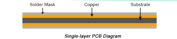
A single-sided PCB features conductive copper traces on one side of a non-conductive substrate, typically fiberglass. This design simplifies manufacturing and minimizes costs, making it ideal for basic electronics with straightforward circuit requirements. However, its limited surface area restricts circuit density, making it less suitable for complex designs. Common applications include remote controls, simple calculators, and basic home appliances.
Double-sided PCB
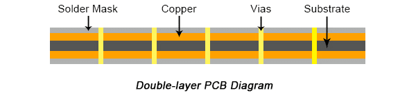
Double-sided PCBs have copper traces on both sides of the substrate, connected through vias (small holes filled with conductive material). This configuration doubles the design space compared to single-sided boards, enabling more complex circuits while reducing electromagnetic interference. Though more expensive, double-sided PCBs offer a balance of performance and cost, suiting applications like consumer electronics, automotive dashboards, and power supplies.
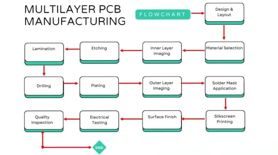
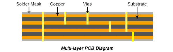
Multilayer PCB
Multilayer PCBs consist of three or more conductive layers, laminated together with insulating material. They support high-density circuits, making them essential for advanced electronics requiring compact designs and robust performance. Despite higher costs and manufacturing complexity, multilayer PCBs are widely used in smartphones, medical devices, and aerospace systems. Their layered structure enhances signal integrity and supports intricate wiring.
The following table compares these PCB types:
PCB Type | Layers | Advantages | Applications | Cost |
---|---|---|---|---|
Single-sided | 1 | Low cost, simple manufacturing | Remote controls, basic appliances | Low |
Double-sided | 2 | Moderate complexity, reduced EMI | Consumer electronics, automotive | Medium |
Multilayer | 3+ | High density, compact design | Smartphones, medical devices | High |
Choosing the right layer count depends on your project’s circuit complexity and budget.
Classification by Substrate Material: Rigid, Flexible, and Rigid-Flex PCBs
The substrate material of a PCB defines its mechanical properties, influencing its suitability for specific applications. PCBs are classified into rigid, flexible, and rigid-flex types based on their base materials, each offering unique characteristics for diverse design needs.
Rigid PCB
Rigid PCBs use solid, non-bendable substrates like FR-4 (fiberglass with epoxy resin), CEM-1, CEM-3, or metal-based materials such as aluminum or copper. These boards provide excellent mechanical strength and stability, making them ideal for fixed installations. FR-4 is the most common, offering robust electrical insulation and durability. Metal-based rigid PCBs, like aluminum substrates, excel in heat dissipation, widely used in LED lighting and power electronics. Rigid PCBs are cost-effective for standard applications but lack flexibility for compact or dynamic designs.
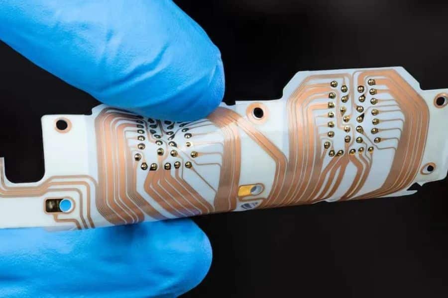
Flexible PCB (FPC)
Flexible PCBs, or FPCs, are made from pliable materials like polyimide or polyester films, allowing them to bend and conform to unique shapes. This flexibility enables compact and lightweight designs, perfect for space-constrained devices. Flexible PCBs are highly durable against vibrations but are more expensive due to specialized materials and manufacturing. They are commonly found in wearable devices, foldable smartphones, and medical implants.
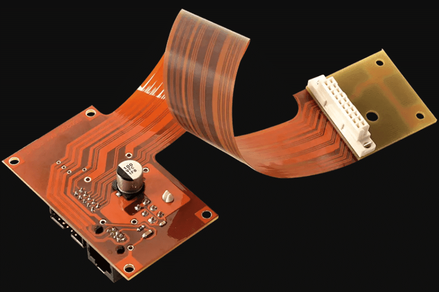
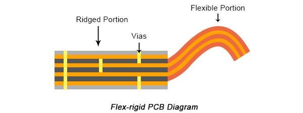
Rigid-Flex PCB
Rigid-flex PCBs combine rigid and flexible substrates, integrating the durability of rigid boards with the adaptability of flexible ones. This hybrid design supports complex, three-dimensional configurations, reducing the need for connectors and saving space. Despite higher costs and manufacturing complexity, rigid-flex PCBs enhance reliability in demanding applications like aerospace, medical devices, and automotive electronics.
The following table compares these PCB types:
PCB Type | Substrate Material | Advantages | Applications | Cost |
---|---|---|---|---|
Rigid | FR-4, aluminum, CEM-1/3 | Durable, cost-effective | LED lighting, power electronics | Low-Medium |
Flexible | Polyimide, polyester | Bendable, lightweight | Wearables, foldable phones | Medium-High |
Rigid-Flex | Rigid + flexible combined | Space-saving, reliable | Aerospace, medical devices | High |
Selecting the right substrate depends on your project’s mechanical and spatial requirements.
Classification by Application Scope: High-frequency and Low-frequency PCBs
PCBs are also classified based on their application scope, particularly the frequency of signals they handle. This categorization divides PCBs into high-frequency and low-frequency types, each tailored to specific performance requirements and industries.
High-frequency PCB
High-frequency PCBs are designed to operate at frequencies above 1 GHz, featuring materials with low dielectric constants and minimal signal loss. These boards ensure fast and reliable signal transmission, critical for applications like 5G communication, radar systems, and satellite technology. Their low water absorption makes them suitable for humid environments, but they require specialized materials, increasing costs. High-frequency PCBs are essential in modern telecommunications and high-speed data processing, where signal integrity is paramount.
Low-frequency PCB
Low-frequency PCBs operate at frequencies below 1 GHz, using standard materials like FR-4. They are cost-effective and simpler to manufacture, making them ideal for applications with less demanding signal requirements, such as household appliances, basic consumer electronics, and industrial controls. While reliable for straightforward designs, low-frequency PCBs may not support high-speed or high-frequency applications due to signal degradation risks.
The following table compares these PCB types:
PCB Type | Frequency Range | Advantages | Applications | Cost |
---|---|---|---|---|
High-frequency | >1 GHz | Fast signal transmission, low signal loss | 5G, radar, satellite systems | High |
Low-frequency | <1 GHz | Cost-effective, easy to manufacture | Appliances, basic electronics | Low |
Selecting the right PCB based on application scope ensures optimal signal performance for your project.
Introduction to PCB Manufacturing Process
The manufacturing process of a PCB transforms raw materials into a functional platform for electronic components. This intricate process directly impacts the board’s performance, reliability, and suitability for specific applications. Understanding the core steps of PCB production provides insight into how different PCB types are crafted to meet diverse design needs.
PCB manufacturing begins with circuit design, where engineers create a digital layout using CAD software to define the electrical pathways. This is followed by photolithography, where a photoresist layer is applied to a copper-clad substrate, and UV light exposes the circuit pattern. Etching removes excess copper, leaving precise conductive traces. For multilayer boards, lamination bonds multiple layers with insulating material. Drilling creates vias for interlayer connections, and plating applies copper to these holes to ensure conductivity. Finally, a solder mask and surface finish are added to protect the board and enhance component soldering.
Each step is tailored to the PCB type, whether single-sided, multilayer, or flexible. High-quality manufacturing ensures durability and performance, critical for applications from consumer electronics to aerospace systems. Learn more about JHYPCB’s advanced PCB manufacturing services for reliable, custom solutions.

How to Choose the Right PCB Type?
Selecting the right PCB type is critical for balancing performance, cost, and design requirements. The choice depends on several factors: circuit complexity, space constraints, environmental conditions, and budget. Below, we outline key considerations and provide practical guidance to help you make an informed decision, supported by real-world examples.
Key Considerations for PCB Selection
- Circuit Complexity: Simple circuits, like those in basic remote controls, can use single-sided PCBs for cost savings. Moderately complex designs, such as automotive sensors, benefit from double-sided PCBs, while advanced applications like smartphones require multilayer PCBs for high-density wiring.
- Space and Weight: Compact devices, such as wearable fitness trackers, demand flexible PCBs to fit tight spaces. Rigid-flex PCBs suit complex, space-constrained products like medical implants, combining durability and adaptability.
- Environmental Conditions: High-frequency PCBs are ideal for 5G devices, ensuring reliable signal transmission in high-speed environments. For high-heat applications like LED lighting, rigid aluminum PCBs offer superior thermal management.
- Budget: Single-sided and low-frequency PCBs minimize costs for budget-sensitive projects, while multilayer or rigid-flex PCBs are pricier but essential for high-performance needs.
Case Studies
- LED Lighting Project: A lighting manufacturer chose a rigid aluminum PCB for its excellent heat dissipation, ensuring long-lasting LED performance in high-temperature environments.
- Wearable Device: A smartwatch developer opted for a flexible PCB to accommodate the device’s curved design, enabling a lightweight and compact product.
By evaluating these factors, you can align your PCB choice with project goals.
Frequently Asked Questions
To help you better understand PCB classification and selection, we’ve compiled answers to common questions about PCBs. These address key concerns for engineers, designers, and project managers.
What is a PCB, and why is classification important?
A PCB is a platform that connects electronic components using conductive copper traces on a non-conductive substrate. Classification—based on layer count, substrate material, and application scope—guides the selection of the right PCB type to optimize performance, cost, and design for specific projects, such as consumer electronics or medical devices.
How do single-sided and double-sided PCBs differ?
Single-sided PCBs have circuits on one side, ideal for low-cost, simple designs like basic appliances. Double-sided PCBs feature circuits on both sides, offering greater design flexibility and reduced electromagnetic interference, suitable for automotive electronics and power supplies.
What are the advantages of rigid vs. flexible PCBs?
When should I use a high-frequency PCB?
High-frequency PCBs, designed for signals above 1 GHz, are ideal for applications requiring fast signal transmission, such as 5G networks and radar systems. Their low dielectric constant ensures minimal signal loss, but they require specialized materials, increasing costs.
For more answers or tailored advice, visit JHYPCB’s FAQ page to explore our expertise in PCB solutions.
Conclusion
Understanding PCB classification is essential for optimizing your electronic projects. By categorizing PCBs based on layer count, substrate material, and application scope, you can select the ideal type—whether a cost-effective single-sided PCB, a flexible PCB for compact designs, or a high-frequency PCB for advanced communication systems. Each classification impacts performance, cost, and reliability, enabling tailored solutions for applications from consumer electronics to aerospace.
JHYPCB offers comprehensive PCB manufacturing services, supporting everything from single-sided boards to 32-layer multilayer designs, rigid to rigid-flex configurations, and high-frequency boards for cutting-edge applications. Our expertise ensures high-quality, customized PCBs that meet your project’s unique requirements. Ready to bring your design to life? Request a free quote or contact our team for expert guidance today!
Advanced Learning:
- Single-layer PCB vs. Double-sided PCB: How to Choose?
- What is a Multilayer PCB and What are the Advantages?
- The Application of Thermoelectric Separated Copper Core PCB in the Field of LED Heat Dissipation
- Key Process Flow of Rigid-Fled PCB Production
- Knowledge of Flexible Printed Circuit Board Processing Technology
- Finding the Right China PCB Manufacturers:5 Vetting Tips
- Guide to Multilayer PCB Layer Stackup and thickness
- What is the Tg value of PCB substrate?
More Adventures: